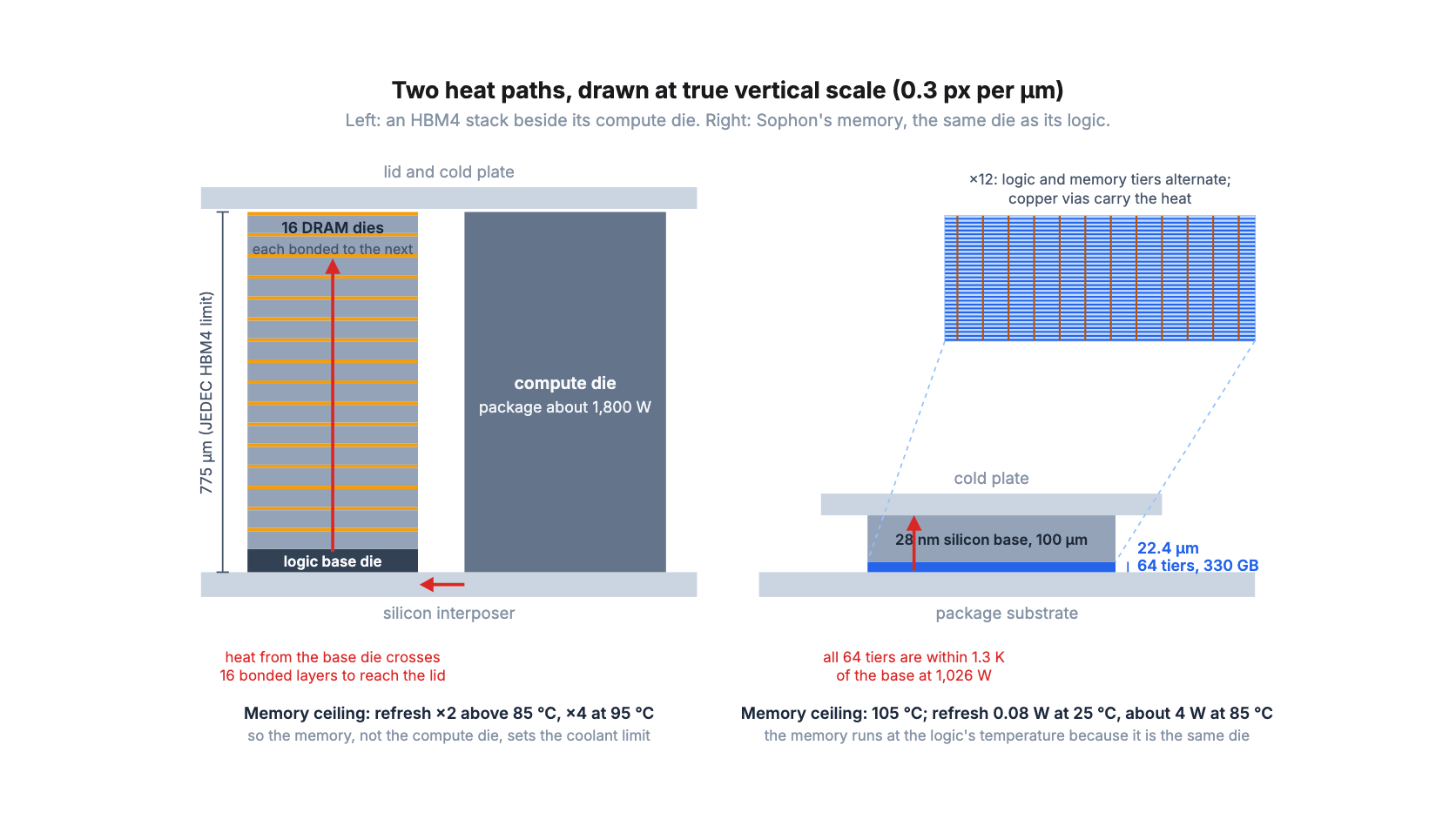
A chip's thermal problem has three parts: how much heat it makes, how far that heat travels to reach the coolant, and what temperature the parts along the way can stand. An HBM GPU and Sophon, our chip design, answer all three differently, and the differences come from one decision. On a GPU the memory is a separate product, a stack of DRAM dies bought from a memory maker and set beside the compute die on an interposer. On Sophon the memory is grown on the same die as the logic, in 64 tiers above a 28 nm silicon base. This post walks the heat from where it is made to where it leaves, on both, with the numbers from whitepaper §6.
Less heat to begin with
Heat is what energy becomes once the work is done, so a chip that spends less energy on a token has less to shed for it. At batch one, where each token must read the whole model, Sophon writes a token for 25.8 mJ, about 174× less than a GPU, which streams every weight out of HBM and across the interposer for each token it writes. Where that number comes from is the distance the weights travel: microns on Sophon, millimeters on a GPU. Per die, Sophon draws 373 W at FP8 decode and 681 W in a peak burst, against about 1,800 W for NVIDIA's Rubin with 288 GB of HBM4 and about 1,700 W for AMD's MI455X with 432 GB. Idle, holding a model resident, Sophon draws about 3 W; an HBM4 subsystem of that size spends 10 to 15 W in self-refresh alone.
One honest qualification before the geometry. GPUs serve many requests at once, and a weight fetched from HBM is shared across the whole batch, so at a full batch the gap in energy per token narrows to about 1.3× against Rubin. The 174× is a batch-one figure. What follows is about where the heat is made and what it has to cross, and that does not change with batch.
775 microns of bonded dies, or 22 of tiers
An HBM stack is twelve or sixteen DRAM dies over a logic base die that carries the interface to the GPU. To fit twelve dies under the old 720 µm limit, SK hynix thinned its DRAM by 40%; for HBM4, JEDEC raised the height to 775 µm for both twelve- and sixteen-high stacks so that the dies could still be joined with microbumps. Between each pair of dies sits a layer of bumps and underfill, or a non-conductive film. Heat made in the base die, the busiest silicon in the stack, crosses every layer above it to reach the lid, and the compute die's heat arrives sideways through the interposer the two share. The memory makers describe the problem in their own numbers. SK hynix says hybrid bonding, which removes the bumps, lowers a stack's thermal resistance by 35%, and that a thermally conductive insulator placed beside the die-to-die interface hotspot takes off another 30%. Analysts expect heat, not bonding, to cap stacks near twenty dies.
Sophon's memory is the same die as its logic. Its 64 tiers, logic and memory alternating, are 0.35 µm each, 22.4 µm in all, grown on a 100 µm silicon base. Vertical copper vias take 6% of the stack's area, and because copper conducts heat about two hundred times better than the dielectric around it, that 6% sets the stack's vertical conductivity at 24.7 W/m·K. Across 22.4 µm and 7.5 cm² of die, that is 0.0012 K/W. The cold plate sits on the back of the silicon base, so the tier farthest from it is the warmest; the whitepaper's per-tier profile, with the dielectric specified as the aluminium oxide the process actually deposits, runs from 48.6 °C at the base to 49.2 °C at the top tier at the 472 W training average, and from 76.3 °C to 77.6 °C at the 1,026 W peak. The whole stack is within 1.3 K of its base. The cold plate's own resistance, 0.05 K/W, is forty times that, so the stack is thermally invisible and a better cold plate improves the whole die at once.
A memory that lives at the logic's temperature
A DRAM cell stores its bit on a capacitor, and the capacitor leaks faster as it warms, about twice as fast for every 10 °C. JEDEC's rule follows the physics: the normal refresh interval holds to 85 °C, and between 85 and 95 °C the memory must be refreshed twice as often; in HBM2 the rate rises to four times at 95 °C. Each refresh is time the array cannot spend serving reads, and it is power: an HBM4 memory of 288 to 432 GB spends 10 to 15 W in self-refresh while the GPU does nothing. This is why GPU monitoring tools report the memory's temperature separately from the die's, and why the coolant limit of an HBM GPU is set by its memory, the component with the lower ceiling, which also happens to stand next to the hottest thing in the package.
Sophon's 2T0C cell has no capacitor. The bit is charge on the gate of one transistor, read through a second, and it leaks with heat at the same rate as DRAM: retention is 1.8 s at 25 °C, 159 ms at 60 °C and 28 ms at 85 °C. The difference is what a refresh costs. With an off-current of 1 fA/µm, refreshing all 330 GB once a second takes 0.08 W. As the die warms, the on-die controller shortens the interval, to 20 ms at 85 °C, and the bill rises to about 4 W, under a 105 °C ceiling. There is no fast-refresh penalty worth counting, and no second component that has to be kept cooler than the logic, because the memory is at the logic's temperature by construction.
What a standard cold plate does with it
On a datacenter cold plate at 0.05 K/W with 25 °C coolant, FP8 decode at 373 W runs at 44 °C, the 681 W peak burst at 60 °C, the 472 W training average at 49 °C, and the 1,026 W forward-plus-backward peak at 78 °C, all below the 105 °C ceiling. The same plate sustains about 1,600 W of this die; microfluidic cooling at 0.02 K/W would sustain about 4,000 W and two-phase immersion about 8,000 W. Air does not do it: a 1U air path at 0.30 K/W would put decode near 137 °C, so Sophon is a liquid-cooled part like the accelerators it competes with, within reach of air only at reduced clocks in an edge box.
What the headroom buys
Forty kelvin of room between decode and the 85 °C the cell tolerates for 4 W is room to run the coolant warm. On Earth, warmer water means less chiller work and heat that is worth recovering; an HBM GPU has to keep its memory under the refresh knee, so its water has to be colder. In orbit, where heat leaves only as radiation, a radiator's area falls with the fourth power of its temperature, which is why the Terafab post prices the whole 2T0C array at 85 °C for about 4 W. And a single die on a substrate has fewer things to break: no interposer, no HBM package, no field of microbumps between memory dies to work loose under thermal cycling.
What this does not say
Sophon's figures are modeled engineering targets from a complete published design, not measurements from shipping silicon; the whitepaper carries every equation and every risk in the open. The thermal model is a lumped network, and the whitepaper calls its stack figures conservative on two counts: it routes the full die power through the stack, where in fact the heat is made across all 64 tiers, and it credits the dielectric with no more than 1.8 W/m·K. The cold plate's 0.05 K/W is a published class figure for the technology, not a measurement of our package, which is still ahead of us.
The memory makers are not standing still. Hybrid bonding, thinner fills and cooling structures beside the hotspot each take tens of percent off an HBM stack's thermal resistance. None of them moves the refresh knee at 85 °C, and none moves the memory away from the compute die it sits beside. Those two facts are the structure of the problem, and they are what a memory grown on the logic's own die does not have.
Frequently asked questions
- Does Sophon need liquid cooling?
- Yes. At 373 W, FP8 decode would reach about 137 °C on a 1U air path at 0.30 K/W, above the 105 °C ceiling. On a standard liquid cold plate at 0.05 K/W it runs at 44 °C, and the plate sustains about 1,600 W of the die. The accelerators it competes with are liquid-cooled too.
- Isn't a 64-tier stack harder to cool than a 16-die HBM stack?
- It is thinner, not thicker. Sixty-four tiers at 0.35 µm are 22.4 µm in all, against 775 µm for an HBM4 stack, and the copper vias that make up 6% of the tiers' area conduct the heat. The modeled rise from the base to the top tier is 0.6 K at 472 W and 1.3 K at 1,026 W; the cold plate's 0.05 K/W is forty times the stack's resistance.
- Why does the memory's temperature set a GPU's cooling limit?
- DRAM leaks faster as it warms, so JEDEC requires refresh twice as often above 85 °C, and HBM2 four times as often at 95 °C. Refresh takes time from reads and burns power, so the memory, which sits beside the compute die, is the part with the lower ceiling. Sophon's cell loses retention at the same rate, but refreshing 330 GB costs 0.08 W at 25 °C and about 4 W at 85 °C, under a 105 °C ceiling, so nothing on the die needs to be cooler than the logic.
- Which tier of Sophon is the hottest?
- The one farthest from the cold plate, which sits on the back of the silicon base. In the whitepaper's per-tier profile it is 49.2 °C at the 472 W training average and 77.6 °C at the 1,026 W peak, 0.6 K and 1.3 K above the base.
References
PhantaField, ‘PhantaField Sophon Whitepaper,’ Rev 4.2, October 2026 — §6, thermal analysis: Figure 11, Eq. 15 (effective vertical conductivity) and Eq. 16 (junction temperature), the cooling-technology table, and the per-tier temperature profile with an Al₂O₃ inter-tier dielectric; §2.B, retention and refresh versus temperature; §5.A.5c, tokens per joule versus batch size. phantafield.com/whitepaper
JEDEC, JESD270-4, High Bandwidth Memory (HBM4), April 2025. The 775 µm package height for 12-high and 16-high stacks, and the earlier 720 µm limit, as reported by ZDNet Korea and TrendForce (April 2025), Blocks and Files (July 2024) and Digital Today.
ServeTheHome, ‘New 36GB SK hynix HBM3E 12-High in Volume Production,’ September 2024 — DRAM dies 40% thinner to hold the 8-high height.
ServeTheHome, ‘SK hynix HBM Packaging at Hot Chips 2026’ — hybrid bonding lowering stack thermal resistance by 35%; the iHBM insulator beside the die-to-die hotspot, over 30%; XenoSpectrum, ‘SK hynix HBM packaging roadmap.’
TrendForce, press release, 30 October 2024 — thermal management as the binding constraint on HBM stack height.
Intel, support article 000076386, Stratix 10 HBM2 — refresh twice as frequent at 85 °C and four times at 95 °C against the 7.8 µs standard interval; SK hynix DDR4 datasheets — extended temperature range 85 to 95 °C, refresh interval halved to 3.9 µs.
Netdata, ‘NVIDIA GPU HBM memory temperature,’ guide, accessed October 2026 — the memory temperature reported separately from the die's (temperature.memory).