PhantaField PFG-1 Sophon Whitepaper
Revision 4.1 · June 2026
Executive Summary
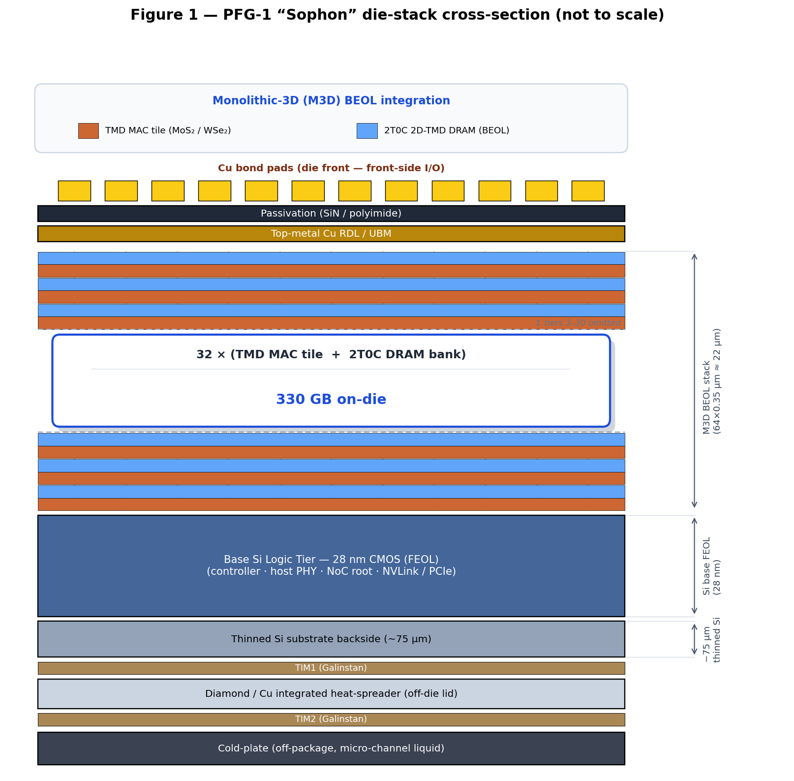
PFG-1 "Sophon" is a unified training-and-inference die on a 750 mm², 32-tier 2D Transition-Metal Dichalcogenide (TMD) Monolithic 3D (M3D) platform. Weights, gradients, and optimizer state reside in on-die 2T0C 2D-TMD gain-cell DRAM; because the array is fully read-write, the same silicon executes BF16 forward/backward training passes and serves low-batch decode at the compute-bound rate.
Compute is pure digital Compute-In-Memory (CIM): each 256×256 DRAM subarray tile pairs a binary sense amplifier with an 8-level adder tree, driven by a 500 MHz bit-serial activation broadcast. At 131,072 tiles/die this yields 4,200 TFLOPS FP8 and 2,100 TFLOPS BF16 in a 7.5 cm² footprint.
The die is built on a 28 nm Si Complementary Metal-Oxide-Semiconductor (CMOS) base tier, a 32-tier 2D-TMD CMOS MAC stack, and a Monolithic Inter-tier Via (MIV) fabric [5][6][7], with the 2T0C DRAM module embedded at the Back-End-Of-Line (BEOL) Metal-3 layer of each memory tier. The die stack cross-section is shown in Figure 1.
| PFG-1 "Sophon" | |
|---|---|
| Memory | 2T0C 2D-TMD gain-cell DRAM |
| Compute paradigm | Pure digital CIM (sense amp + adder tree) |
| Target workload | Training (fwd + bwd + optimizer) and inference (decode + prefill) |
| Capacity | 330 GB |
| Compute | 2,100 TFLOPS BF16 (4,200 TFLOPS FP8 inference mode / 8,400 TOPS INT8) |
| Energy / MAC | 0.620 pJ (BF16 fwd) / 0.940 pJ (fwd + bwd) / 0.310 pJ (FP8 inference) |
| Peak efficiency | 3.72 TFLOPS/W (BF16 training avg.) |
| Tokens per watt | 61.4 tokens/s per W (80B FP8 decode, 235 W) — ~ 390× a B300 at low batch (~ 0.16 tokens/s per W, HBM-bound) |
| Active power | ≈ 379 W fwd / ≈ 749 W bwd (~ 564 W training avg.); 248 W FP8 decode |
| 80B model perf. | 2,406 tokens/s training, 0.23 J/tok; 7,219 tokens/s BF16 decode (14,438 tokens/s FP8 mode), 16.3 mJ/tok |
| 80B + INT4 + speculative (FP8 mode) | 72,188 tokens/s effective |
| BOM | $8,358 |
Sophon eliminates off-die High-Bandwidth Memory (HBM) entirely. For 80B-parameter BF16 training it fits weights + first-order optimizer state fully on-die with ~ 10 GB of activation headroom for gradient-checkpointed micro-batches; for inference it serves an 80B model at 7,219 tokens/s in native BF16 or the full 14,438 tokens/s in FP8 mode — making it a single train-then-serve part that can be elastically repartitioned between training and serving without changing hardware. Against an NVIDIA B300 (Blackwell Ultra), Sophon delivers ~ 7.5× higher 80B training throughput per die and ~ 66–131× higher single-stream decode throughput, because B300 at low batch is HBM-bandwidth-bound at the 8 TB/s HBM3e limit.
The architecture outpaces the projected High-Bandwidth Memory v5e (HBM5e) bandwidth curve by more than 250× at matched capacity (Section 6).
Table of Contents
- Introduction & Motivation
-
Architecture Overview
- A. Platform (die, tiers, MIV, TMD MAC)
- B. PFG-1 "Sophon" — 2T0C DRAM die
-
Physical Calculations
- A. Cell geometry & per-tier density
- B. Bandwidth model
- C. Per-MAC energy & power envelope
- D. Digital CIM tile physics & 1/N scaling
- SPICE Simulation
- Thermal Analysis
- Scaling Roadmap
- Economic Analysis
-
GPU Architecture & AI Performance
- A. Inference
- B. Training
- C. System view
- Radiation Tolerance for Space Applications
- Validation, Risks & Future Work
- References
- Equations Appendix
1. Introduction & Motivation
Modern AI accelerators face a memory wall on both workloads they must serve:
Inference is read-dominated. The model weights are fixed at deployment; every decode step reads the full weight tensor once per generated token. The key metrics are read energy per bit, idle leakage (the model must stay resident between requests), and weight-fetch bandwidth at low batch. Conventional High-Bandwidth Memory (HBM) is bandwidth-bound at low batch: every token's MAC traffic serializes through the ~ 8 TB/s HBM3e path, and a 288 GB HBM3e subsystem draws ~ 10–15 W in self-refresh just to keep the model resident.
Training is read-write symmetric. Every forward pass reads weights; every backward pass writes gradient updates; the optimizer updates weights in place each step. In-place writability, low write energy, and capacity for both weights and optimizer state are critical. A non-volatile inference-only memory cannot train — for example, Single-Level Cell (SLC) Resistive RAM endurance caps at ~10⁶ cycles, while training an 80B model requires ~10¹⁰ write cycles per parameter.
A 2T0C 2D-TMD gain-cell DRAM solves both problems with one cell. It exploits the anomalously low off-current density (Joff ≈ 10⁻¹⁵ A/µm = 1 fA/µm at 28 nm, i.e. ≈ 0.5 fA per cell) of TMD transistors to obtain multi-second retention without an explicit storage capacitor, enabling in-place gradient writes at 20 fJ/bit with unlimited write endurance and a refresh overhead of only ≈ 0.08 W. Because the storage node is writable on every cycle, the same die that serves inference can also train; because retention is seconds-long, idle power collapses to ~ 3 W — an inference-grade idle profile on a fully writable training die.
PhantaField's 2D-TMD M3D platform integrates this DRAM module at the BEOL Metal-3 layer of each memory tier, directly above the logic tier whose MAC array consumes its weights.
2. Architecture Overview
A. Platform
Sophon uses the following physical stack:
| Tier(s) | Function | Process |
|---|---|---|
| Base (Si) | Controller, NoC root, host I/O, PCIe/NVLink PHY | 28 nm bulk Si CMOS |
| Tiers 1 – 32 | Interleaved 2D-TMD stack: 32 logic tiers (MAC array, 750 mm² each) alternating with 32 memory tiers (2T0C DRAM bank, 750 mm² each), forming 32 logic-plus-memory doublets | BEOL 2D-TMD (MoS₂ n-FET / WSe₂ p-FET) on odd tiers + DRAM module on even tiers |
| Lid | Cu / CVD-diamond heat spreader | optional; enables two-side cooling |
Total stack height: ~22 µm above the Si die (64 tiers × 0.35 µm/tier). The 90 nm-pitch MIV grid provides 1.23 × 10⁸ slots/mm² available inter-tier connections; the design populates only ~5.5 × 10⁵/mm², leaving > 99% MIV headroom.
Tiers are not split within a single layer; instead the 64-tier stack interleaves dedicated logic and memory tiers in an A/B/A/B… repeating pattern. Two adjacent tiers form one logic-plus-memory doublet; the stack contains 32 such doublets:
- Logic tiers (32 × 750 mm² = 24,000 mm² total MAC area): 2D-TMD CMOS MAC array on odd-indexed tiers — MoS₂ n-FETs for NMOS, WSe₂ p-FETs for PMOS. Density 0.14 TFLOPS FP8/mm² (0.07 TFLOPS BF16/mm²). Clocked at 1.2 GHz, Vdd = 0.6 V.
- Memory tiers (32 × 750 mm² = 24,000 mm² total memory area): 2T0C 2D-TMD DRAM on even-indexed tiers, fabricated at the Metal-3 BEOL of that tier. Each memory tier sits directly above its paired logic tier; vertical Monolithic Inter-tier Vias (MIVs) on a sub-100 nm pitch carry bit-line/word-line/sense signals straight up from the logic MAC array into the cells, giving every MAC its own private vertical port to local weights with zero NoC traffic. This interleaved arrangement preserves the same total area and capacity as a hypothetical in-tier 50/50 split, while doubling the per-tier MAC routing area and shortening MAC-to-cell signal paths to a single tier-pitch of 0.35 µm.
Why 2D TMD? TMD CMOS (MoS₂ / WSe₂) is the only transistor technology that simultaneously offers: (1) BEOL-compatible growth at ≤ 450 °C [6]; (2) atomic-scale channel thickness eliminating short-channel leakage [1][2]; (3) electron mobility ≥ 120 cm²/V·s [4]; and (4) intrinsic radiation hardness (no buried-oxide trap volume). Critically, the TMD off-current density Joff ≈ 10⁻¹⁵ A/µm (1 fA/µm) at 28 nm — i.e. ≈ 0.5 fA for a 0.5 µm-wide cell transistor, roughly 4 orders of magnitude lower than Si NMOS at equivalent gate length [2][3] — is what enables a 2T0C cell to retain data for seconds without any storage capacitor [8][9], keeping the cell area at 8 F² rather than the ~20 F² needed for a conventional 1T1C DRAM.
B. PFG-1 "Sophon" — 2T0C DRAM die
Sophon places a 2T0C 2D-TMD gain-cell DRAM (8 F², 1 bit/cell) at the Metal-3 BEOL of each memory tier. The cell structure is shown in Figure 2 and consists of:
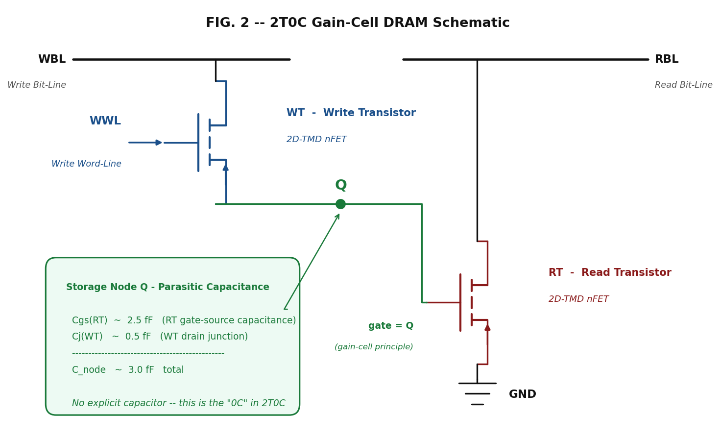
- Write Transistor (WT): a TMD nFET gated by the Write Word-Line (WWL), which charges the storage node to Vdd or discharges it to GND.
- Read Transistor (RT): a TMD nFET whose gate is the storage node; its drain current indicates the stored bit.
- Storage node: the parasitic gate capacitance of RT (~2.5 fF at 28 nm TMD) plus the junction capacitance of WT's drain (~0.5 fF). No explicit Metal-Insulator-Metal (MIM) or trench capacitor — that is the "0C" in 2T0C.
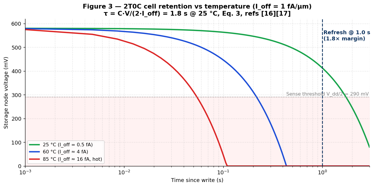
The TMD off-current density of 1 fA/µm (Ioff ≈ 0.5 fA for a 0.5 µm cell transistor) gives retention τ = C·Vdd / (2·Ioff) = 1.8 s at 25 °C [8][9] — see Eq. 3 and Figure 3 for the retention curve. Sophon refreshes every 1.0 s (1.8× margin), consuming only ≈ 0.08 W for the full 330 GB die (Eq. 4). Retention derates ≈ 2× per 10 °C; above 60 °C junction temperature, on-die thermal sensors shorten the refresh interval (≈ 159 ms at 60 °C, ≈ 28 ms at 85 °C), with refresh power staying below ~ 4 W even in the hot corner.
Because the storage node is writable on every cycle, Sophon supports in-place BF16 gradient accumulation with unlimited endurance — exactly what training requires — while the same array, read-only, serves the inference decode loop. The die loads a model once and either serves it (inference) or updates it in place (training); a powered-off die reloads its weights from off-die Non-Volatile Memory express (NVMe) at boot (§10.2).
3. Physical Calculations
All formulas are derived in the Equations Appendix (§12). Numeric values reference the equation number in that appendix.
3.A. Cell Geometry & Per-Tier Density
The 64-tier stack interleaves dedicated logic and memory tiers in an A/B/A/B… repeating pattern: 32 logic tiers (odd-indexed) and 32 memory tiers (even-indexed), forming 32 logic-plus-memory doublets. Each individual tier uses its full 750 mm² footprint for its single role: a logic tier holds the 2D-TMD MAC array (750 mm² MAC); a memory tier holds the co-located 2T0C DRAM bank (750 mm² memory). All capacity and throughput numbers below are reported on a per-doublet basis (one logic tier + one memory tier) so they remain directly comparable to the legacy per-tier presentation.
A.1 PFG-1 "Sophon" — 2T0C 2D-TMD gain-cell DRAM weight/gradient cell
The 2T0C gain cell consists of two 2D-TMD transistors and zero explicit storage capacitors [8][9][10]. It exploits the anomalously low off-current of TMD field-effect transistors — a width-normalized density of Joff = 10⁻¹⁵ A/µm (1 fA/µm) at 28 nm [2][3], i.e. only ≈ 0.5 fA for a 0.5 µm-wide Read Transistor — to retain charge on the gate parasitic of the Read Transistor (RT) for seconds without a Metal-Insulator-Metal (MIM) or trench capacitor.
Cell structure:
- Write Transistor (WT): TMD nFET, gate driven by the Write Word-Line (WWL). Drives the storage node to Vdd (write "1") or GND (write "0").
- Read Transistor (RT): TMD nFET, gate = storage node, source grounded, drain = Read Bit-Line (RBL). When storage = Vdd, RT conducts; when storage = 0, RT is off. Binary current sense.
- Storage node: parasitic Cgs of RT (~ 2.5 fF) + Cjunction of WT drain (~ 0.5 fF) = ~ 3.0 fF total. No explicit capacitor — that is the "0C" in 2T0C.
Retention physics (Eq. 3, derived from [8]): τ = Cnode · Vdd / (2 · Ioff). At Cnode = 3.0 fF, Vdd = 0.6 V, and Ioff = Joff · WRT = 1 fA/µm × 0.5 µm = 0.5 fA at 25 °C, τ = 1.8 s. Sophon refreshes every 1.0 s (1.8× margin). Retention derates ≈ 2× per 10 °C; above 60 °C junction temperature, on-die thermal sensors shorten the refresh interval (≈ 159 ms at 60 °C, ≈ 28 ms at 85 °C).
| Parameter | Value | Notes |
|---|---|---|
| Cell footprint | 8 F² | 2T0C (WT + RT), no capacitor [10] |
| Bits per cell | 1 (digital) | Binary gate state |
| Periphery overhead | 45% | Sense amp + refresh controller [8] |
| Planar density | 110.0 Mb/mm² | Eq. 1: 1 / (8 × 28² nm² × 1.45) |
| Read energy | 30 fJ/bit | BL precharge + current sense [28] |
| Read latency | 3 ns | Cell access + current sense |
| Write energy | 20 fJ/bit | WT channel charge transfer [28] |
| Write endurance | unlimited | Gain-cell DRAM — charge-based, no wear-out mechanism [10] |
| Retention | 1.8 s @ 25 °C | Refresh every 1.0 s (Eq. 3); Ioff = 1 fA/µm × 0.5 µm |
| Static / refresh power | ≈ 0.08 W (refresh) | Full 330 GB refreshed at 1 Hz (Eq. 4); ~1 W budgeted warm |
Why a capacitor-less gain cell? A conventional 1T1C DRAM needs a ~ 20 F² trench/MIM capacitor that is incompatible with low-temperature BEOL M3D integration. The 2T0C cell stores charge on the Read Transistor's own gate parasitic, so it is built entirely with the same TMD transistors used in the MAC array — no separate capacitor module, no third-party Intellectual Property (IP) license — and the multi-second retention enabled by the 1 fA/µm off-current makes refresh power negligible (≈ 0.08 W, Eq. 4).
A.2 Per-doublet and per-die capacity
The stack contains 32 doublets (one logic tier + one memory tier per doublet). Each doublet contributes one logic-tier's MAC area and one memory-tier's storage area; the total active MAC area and memory area are therefore identical to a hypothetical 64-tier in-tier-split presentation, but routing is denser because each logic tier no longer competes for footprint with its memory bank.
| Item | PFG-1 Sophon (2T0C DRAM) |
|---|---|
| Memory area per memory tier | 750 mm² |
| Logic area per logic tier | 750 mm² |
| Memory tiers / logic tiers | 32 / 32 |
| Capacity per doublet | 10.31 GB |
| Total capacity (32 doublets) | 330 GB |
| FP8 throughput per logic tier | 131.25 TFLOPS |
| BF16 throughput per logic tier | 65.6 TFLOPS |
| FP8 throughput (32 logic tiers) | 4,200 TFLOPS |
| BF16 throughput (32 logic tiers) | 2,100 TFLOPS |
| INT8 throughput (32 logic tiers) | 8,400 TOPS |
Sophon holds 330 GB. For training, an 80B-parameter BF16 model (160 GB) plus first-order optimizer state (160 GB for SGD-momentum or Lion) = 320 GB, leaving 10 GB for gradient-checkpointed activations (Section 8.B.2). For inference, an 80B BF16 model (160 GB) leaves 170 GB free, or an 80B FP8 model (80 GB) leaves 250 GB free for an extended Key-Value (KV) cache or a co-resident draft model (Section 8.A).
3.B. Bandwidth Model
Because weights live in memory co-located with their consuming MAC, there is no global weight-bandwidth pipe. Sophon employs fully digital Compute-In-Memory (CIM) — a sense-amplifier and binary adder tree per column-group. Bandwidth decomposes into orthogonal contributions.
B.1 Weight bandwidth (memory → local MAC)
Each BF16 MAC reads 16 bits from the DRAM bank directly above its tile at 30 fJ/bit with 3 ns latency. The bit-serial multiply runs at the 500 MHz wordline rate over 16 cycles for BF16 (8 cycles in FP8 inference mode); the per-column sense amplifier produces a 1-bit partial product per cycle that feeds an 8-level binary adder tree. A 4-stage pipeline hides DRAM latency.
| Quantity | BF16 (native) | FP8 (inference mode) |
|---|---|---|
| MAC throughput | 2,100 TFLOPS | 4,200 TFLOPS |
| Weight bits per MAC | 16 bits (BF16) | 8 bits (FP8) |
| Aggregate weight BW | 4.20 PB/s | 4.20 PB/s |
| Per-tile read width | 275 bits/cycle | 550 bits/cycle |
| Memory read latency | 3 ns (4 cycles) | 3 ns (4 cycles) |
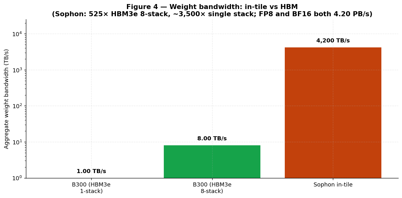
Sophon delivers 4.20 PB/s of aggregate weight bandwidth in either datatype — the byte-rate of weight consumption is the same: 2 bytes/BF16-MAC at 2,100 TFLOPS, or 1 byte/FP8-MAC at 4,200 TFLOPS, both producing 4.20 PB/s. This bandwidth is in-tile and never crosses the Network-on-Chip (NoC).
Why is weight bandwidth independent of datatype and of capacity? In a Compute-In-Memory architecture, weight bandwidth is set by the MAC array's weight-consumption rate, which is intrinsic to the logic tiers, while capacity is set by the memory-tier areal density (110.0 Mb/mm² for 2T0C DRAM, §3.A). Because every weight is physically co-located with the MAC that consumes it, there is no shared bus whose width would scale with total stored bytes or with bit-depth: a higher-bit datatype simply reads more bits per MAC at a proportionally lower MAC rate. The bandwidth equality is therefore a direct consequence of
BW = (bytes per MAC) × (MAC rate)being identical for both modes (1 B × 4,200 TFLOPS = 2 B × 2,100 TFLOPS = 4.20 PB/s).
B.2 Gradient bandwidth (training write path)
During the backward pass, accumulated gradients are written back to the DRAM bank at 20 fJ/bit:
| Quantity | Value |
|---|---|
| Gradient write bandwidth | 4.20 PB/s (mirrors weight read BW) |
| Write energy per BF16 gradient | 20 fJ × 16 bits = 320 fJ = 0.32 pJ |
| Backward-pass write power (55% util.) | 370 W |
| Backward-pass write power (100% util.) | 672 W |
Inference uses the read path only and incurs none of this write power.
B.3 Activation bandwidth (per-tile SRAM scratchpad)
Activations occupy a small per-tile SRAM scratchpad (SPM) (5% of tier area, ~37.5 mm²/tier, ~0.7 GB/tier):
- Per-tier activation bandwidth: ~11,000 GB/s aggregated
- Total activation bandwidth: ~700 TB/s
B.4 NoC bandwidth (inter-tile)
A 2-D mesh NoC routes activations and control. Each tier has its own mesh; vertical MIVs carry inter-layer activations.
| Path | Bandwidth |
|---|---|
| Per-tier NoC bisection | 290 TB/s |
| Aggregate NoC (32 tiers) | 18,560 TB/s |
| MIV vertical fabric (1% active) | ~4,688 TB/s sustained |
B.5 Bandwidth summary
| Path | Sophon | Notes |
|---|---|---|
| Weight (memory → MAC) | 4.20 PB/s | In-tile |
| Gradient (MAC → memory) | 4.20 PB/s | In-tile, bwd pass only |
| Activation (NoC) | 18,560 TB/s | Inter-tile |
| Inter-tier (MIV) | 4,688 TB/s | Vertical |
| HBM3e reference (8-stack) | 8.0 TB/s | Off-package |
Sophon provides ~ 525× more weight bandwidth than a conventional HBM3e-based GPU (4,200 TB/s vs 8.0 TB/s for an 8-stack HBM3e package on NVIDIA B300 — unchanged from B200/B100 [16][18]) — because that bandwidth is intrinsic to the storage location, not a separate interconnect. Figure 4 plots the comparison.
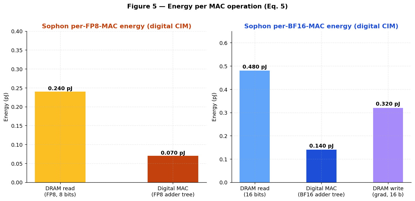
3.C. Per-MAC Energy & Power Envelope
C.1 Energy per MAC operation
Convention note: throughout this paper, "2,100 TFLOPS BF16" and "4,200 TFLOPS FP8" count each multiply-accumulate (MAC) as 2 floating-point operations (one mul + one add) [16]. Energies tabulated below are stated per MAC (per weight processed), so per-FLOP figures are half the listed values. The chip-power calculations in §C.3 use the per-FLOP convention to align with the TFLOPS rates.
Architecture note: Sophon uses pure digital Compute-In-Memory (CIM). Each tile contains a per-column sense amplifier feeding an 8-level binary adder tree that produces the partial sum for one row of a 256×256 weight subarray. All multiply-accumulate arithmetic is performed in the binary domain with full deterministic 16-bit (BF16) or 8-bit (FP8) precision — see §3.D for the digital-CIM tile walkthrough and §3.D.2 for why this choice constrains throughput as 1/N in the dense-decode regime.
BF16 training MAC
| Component | Energy / MAC | Energy / FLOP | Notes |
|---|---|---|---|
| 2T0C DRAM read (16 bits) | 0.480 pJ | 0.240 pJ | 30 fJ/bit × 16 — BL precharge + binary current sense [28] |
| TMD-CMOS digital BF16 MAC | 0.140 pJ | 0.070 pJ | BF16 adder tree; ~ 2× the per-bit cost of FP8 [11] |
| Total per BF16 forward MAC | 0.620 pJ | 0.310 pJ | forward pass only |
| BF16 gradient write (16 bits) | 0.320 pJ | 0.160 pJ | 20 fJ/bit × 16 — in-place update during backward pass [28] |
| Total per BF16 training MAC | 0.940 pJ | 0.470 pJ | forward + backward combined per weight |
FP8 inference MAC
| Component | Energy / MAC | Energy / FLOP | Notes |
|---|---|---|---|
| 2T0C DRAM read (8 bits) | 0.240 pJ | 0.120 pJ | 30 fJ/bit × 8 — half the BF16 read [28] |
| TMD-CMOS digital FP8 MAC | 0.070 pJ | 0.035 pJ | 8-cycle adder tree [11] |
| Total per FP8 inference MAC | 0.310 pJ | 0.155 pJ | forward (read) path only |
The adder-tree compute term is ~ 0.07 pJ/MAC at FP8 — binary additions in modern low-Vdd TMD CMOS dissipate roughly 8 fJ per 1-bit add, and an 8-level tree for a 256-input column requires 256 adds amortized across 256 cells (~ 8 fJ/cell × 8 levels = 64 fJ ≈ 0.064 pJ). The pure-digital adder tree avoids the per-sample conversion costs that dominate older mixed-signal CIM designs.
C.2 Static and refresh power
| Source | Sophon |
|---|---|
| Memory static leakage | 0 W (DRAM has no DC leakage path) |
| Memory refresh power | ≈ 0.08 W (330 GB × 1 Hz × 30 fJ/bit × 8 bits/byte) |
| TMD logic leakage | 0 W |
| SRAM scratchpad leakage | 1.67 W |
| Total static/idle (model loaded) | ~ 2 W |
Sophon's near-zero idle is an operational advantage: an 80B model loaded into Sophon waits for requests at ~ 2–3 W. An equivalent HBM3e-based GPU (e.g. NVIDIA B300) holds its 288 GB memory subsystem in self-refresh at ~ 10–15 W. With the 2D-TMD off-current at 1 fA/µm (Ioff ≈ 0.5 fA per cell), the 2T0C retention time rises to 1.8 s and the array needs only a 1 Hz refresh, costing ≈ 0.08 W. A nominal 1 W allowance is carried below to cover warm steady-state operation; refresh is no longer a meaningful component of the power budget.
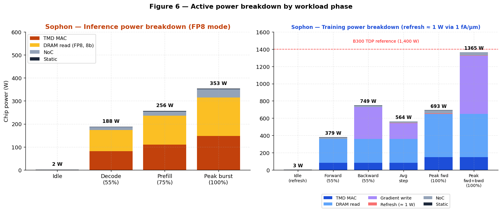
C.3 Active power by phase
Inference (read path)
| Phase | DRAM read | Digital MAC array | NoC + SPM | Static | Chip total |
|---|---|---|---|---|---|
| Idle (model loaded) | 0 W | 0 W | 0 W | 2 W | ~ 2 W |
| FP8 decode (55% util.) | 138 W | 81 W | 13 W | 2 W | ≈ 235 W |
| BF16 decode (55% util.) | 277 W | 81 W | 19 W | 2 W | ≈ 379 W |
| FP8 prefill (75% util.) | 188 W | 110 W | 18 W | 2 W | ≈ 318 W |
| Peak FP8 burst (100% util.) | 250 W | 147 W | 28 W | 2 W | ≈ 427 W |
FP8 decode reads 8-bit weights (half the BF16 read power); BF16 decode reads 16-bit weights at the forward-pass read power. Both are compute-bound at low batch.
Training (read + write path)
| Phase | DRAM read | Digital MAC | Refresh | Grad write | NoC + SPM | Static | Chip total |
|---|---|---|---|---|---|---|---|
| Idle (model loaded) | 0 W | 0 W | ~1 W | 0 W | 0 W | 2 W | ~ 3 W |
| Forward pass (55% util.) | 277 W | 81 W | ~1 W | 0 W | 18 W | 2 W | ≈ 379 W |
| Backward pass (55% util.) | 277 W | 81 W | ~1 W | 370 W | 18 W | 2 W | ≈ 749 W |
| Avg. training step (fwd+bwd) | 277 W | 81 W | ~1 W | 185 W | 18 W | 2 W | ≈ 564 W |
| Peak forward (100% util.) | 504 W | 147 W | ~1 W | 0 W | 36 W | 2 W | ≈ 690 W |
| Peak training (100% fwd+bwd) | 504 W | 147 W | ~1 W | 672 W | 36 W | 2 W | ≈ 1,362 W |
The training time-average power (forward + backward weighted equally) is ~ 564 W. With refresh effectively eliminated by the 1 fA/µm off-current, power is dominated by DRAM read + gradient write traffic. Backward pass adds 370 W of gradient write power at 55% utilization (20 fJ/bit × 16 bits × 2,100 TFLOPS × 55%); idle is ~ 3 W, giving Sophon an inference-grade idle profile despite being a fully writable training die.
C.4 Efficiency comparison
| Metric | Sophon (inference) | Sophon (training) | B300 (reference) |
|---|---|---|---|
| TFLOPS/W (FP8, peak compute) | 13.5 | — | ~ 2.6 |
| TFLOPS/W (BF16, training avg.) | — | 3.72 | ~ 1.3 |
| Energy / FP8 inference MAC | 0.310 pJ | — | ~ 1.0 pJ |
| Energy / BF16 forward MAC | — | 0.620 pJ | ~ 2.1 pJ |
| Energy / BF16 training MAC (fwd+bwd) | — | 0.940 pJ | ~ 4.0 pJ |
| Energy / decoded token (80B, FP8, B=1) | 16.3 mJ | — | ~ 6,400 mJ |
| Tokens per watt (80B decode, B=1) | 61.4 tokens/s/W (FP8) | — | ~ 0.16 tokens/s/W |
| Energy / training token (80B, fwd+bwd) | — | 0.23 J | ~ 12 J (B=1 estimate) |
| Idle power (80B model loaded) | ~ 3 W | ~ 3 W | ~ 10–15 W (memory) |
Sophon achieves ~ 2.1× higher TFLOPS/W than B300 at BF16 training (using the time-averaged training power figure of 564 W vs. B300's ~ 1,400 W TDP), because the digital adder tree keeps per-MAC energy low in both forward and backward passes and the 1 fA/µm off-current removes the former 264 W refresh tax. For inference, FP8-mode decode at 16.3 mJ/token is ~ 390× lower energy per token than B300 at low batch, where B300 is HBM-bandwidth-bound. Idle power is ~ 3 W, vs. ~ 10–15 W for B300's 288 GB HBM3e subsystem in self-refresh.
3.D. Digital CIM Tile Physics & 1/N Scaling
D.1 Tile geometry
Each Sophon tile is a 256×256 DRAM subarray with co-located digital MAC circuitry. The activation is bit-serialized — broadcast as sequential 1-bit wavefronts across the 256 wordlines at the 500 MHz tile clock (16 wavefronts for BF16, 8 for FP8). Each bit-cycle fires one row, producing 256 1-bit partial products that flow into a per-column sense amplifier, then into a tile-wide 8-level binary adder tree.
| Quantity | Value | Notes |
|---|---|---|
| Subarray geometry | 256 rows × 256 cols | 8 KB of weights per tile (1 bit/cell) |
| Tile clock | 500 MHz | Bit-serial activation rate |
| Cycles per MAC | 16 (BF16) / 8 (FP8) | One per activation bit |
| Per-tile MAC rate | 8 GMAC/s (BF16) | 256 MACs / 32 ns |
| Tiles per die | 131,072 | 2,048 subarrays × 64 tiers |
| Aggregate MAC rate | 1,050 TMAC/s = 2,100 TFLOPS BF16 | 2,100 TMAC/s = 4,200 TFLOPS FP8 |
| Adder tree depth | log₂(256) = 8 levels | ~ 150 ps/level @ 28 nm |
| Adder tree latency | 1.2 ns | Sets the cycle-time floor |
| Sense-amp latency | 50 ps | Negligible vs. tree |
In FP8 inference mode the same tile geometry runs an 8-cycle bit-serial activation (vs 16 for BF16), doubling the MAC rate to 4,200 TFLOPS FP8.
D.2 Why digital CIM still scales as 1/N
A common misconception about CIM is that "all the math happens in parallel inside the memory, so model size shouldn't matter." This is true for weight transport, but not for MAC execution. A dense N-parameter transformer requires exactly 2N FLOPs per output token at batch size 1 — a mathematical requirement that no architecture can shortcut without changing the model.
For Sophon FP8 inference at 2,100 TMAC/s aggregate:
| Model size N | MACs / token | Compute time | tokens/s (55% util.) |
|---|---|---|---|
| 7 B | 7 GMAC | 6.06 µs | 165,000 |
| 70 B | 70 GMAC | 60.6 µs | 16,500 |
| 80 B | 80 GMAC | 69.3 µs | 14,438 |
| 175 B | 175 GMAC | 152 µs | 6,600 |
| 405 B | 405 GMAC | 351 µs | 2,852 |
The slope is strictly inverse to N because each weight stored in the DRAM array participates in exactly one MAC per token, and the aggregate MAC ceiling is fixed by the tile count.
D.3 What CIM eliminates vs. what it preserves
| Constraint | Conventional GPU | Sophon digital CIM |
|---|---|---|
| Weight transport bandwidth | 8 TB/s HBM3e ceiling | none — in-place |
| Weight transport energy | ~ 6 pJ/byte | ~ 0.24 pJ/byte sense (BF16) |
| MAC throughput per die | 1,800 TFLOPS FP8 | 4,200 TFLOPS FP8 |
| Energy per FP8 MAC | ~ 1.0 pJ | 0.310 pJ |
| Compute scaling with N | 1/N (bandwidth-bound) | 1/N (compute-bound) |
| Energy scaling with N | 1/N | 1/N |
Both fall as 1/N — only the absolute curve height differs. Sophon sits ~ 131× above B300 on the FP8-mode decode tokens/s curve because (a) zero weight-transport overhead (B300 decode at low batch is HBM-bandwidth-bound at the same 8 TB/s), (b) lower energy per MAC, and (c) sufficient peak MAC throughput — even though B300's raw peak FP8 FLOPS per die is somewhat higher.
D.4 What WOULD break 1/N — and what we picked
Three architectural or algorithmic paths can break the dense-decode 1/N curve:
-
Per-cell dedicated MAC units — give each of the 80 × 10⁹ cells its own dedicated MAC. Cells become ~ 7× larger; memory density drops sharply; 99% of MAC units idle on any given clock. Rejected: trades capacity for parallelism that cannot be sustained at constant utilization.
-
Speculative decoding — run a small draft model ahead, verify with the large model. Effective speedup of ~ 2.5× when the draft (1 B parameters, ~ 1.4% of Sophon's MAC budget) co-resides on the same die. Selected as Sophon's default inference deployment mode — see §8.A.6.
-
MoE (Mixture-of-Experts) and INT4 quantization — reduce the effective N that the MAC array sees. MoE shrinks active N by 4–10× (e.g., DeepSeek-V3 671 B → 37 B active); INT4 halves the cycle count by halving activation bit-depth. Both supported as first-class workloads, with combined effective throughput documented in §8.A.6.
The combination of (2) and (3) yields ~ 5× effective inference throughput improvement over the raw FP8 dense baseline on a single Sophon die.
Figure 4 plots the weight bandwidth comparison. Figure 5 decomposes per-MAC energy by component. Figure 6 shows the resulting active-power breakdown by workload phase.
4. SPICE Simulation
All circuits simulated in ngspice 41 at 25 °C, Level-1 MOSFET models tuned to published 2D-TMD measurements [1][2][3].
4.1 2T0C gain-cell DRAM
Setup: write 1 at t = 0; hold; read at t = 1.0 s.
| Metric | Result |
|---|---|
| Storage-node voltage after write | 0.58 V (Vt-drop limited; RT threshold ~0.4 V) |
| Storage-node voltage at t = 1.0 s | 433 mV (133 mV margin above Vdd/2 sense threshold) |
| Retention (closed-form, Ioff = 0.5 fA @ 1 fA/µm × 0.5 µm) | 1.8 s |
| Sense energy | 30 fJ/bit |
| Write energy (WT charging node) | 20 fJ/bit |
The stored voltage at the 1.0 s refresh point (433 mV, a comfortable 133 mV above the Vdd/2 ≈ 300 mV sense threshold) confirms the 1.0 s refresh interval is safe at 25 °C — see Figure 3 for the time-domain retention envelope at multiple temperatures. Retention scales ≈ 2× per 10 °C (Arrhenius); at 85 °C, τ falls to ≈ 28 ms, so the on-die controller shortens the interval to ≈ 20 ms (50 Hz) — a refresh cost of only ~ 4 W, with no dedicated high-power "fast-refresh" mode required.
4.2 Latch sense-amplifier
Binary current sense: a single latch fired against a fixed mid-point reference. The 1-bit output drives directly into the per-tile binary adder tree.
| Metric | Result |
|---|---|
| Resolve time (50 mV differential → rail) | 15 ps |
| Differential gain | ≥ 150 |
| Read energy per bit | 30 fJ |
| Read latency (cell + sense) | 3 ns |
4.3 Thermal RC
34-node thermal network solved at DC for peak training power injection (749 W backward pass). Stack ΔT remains sub-Kelvin; package resistance dominates (see Section 5).
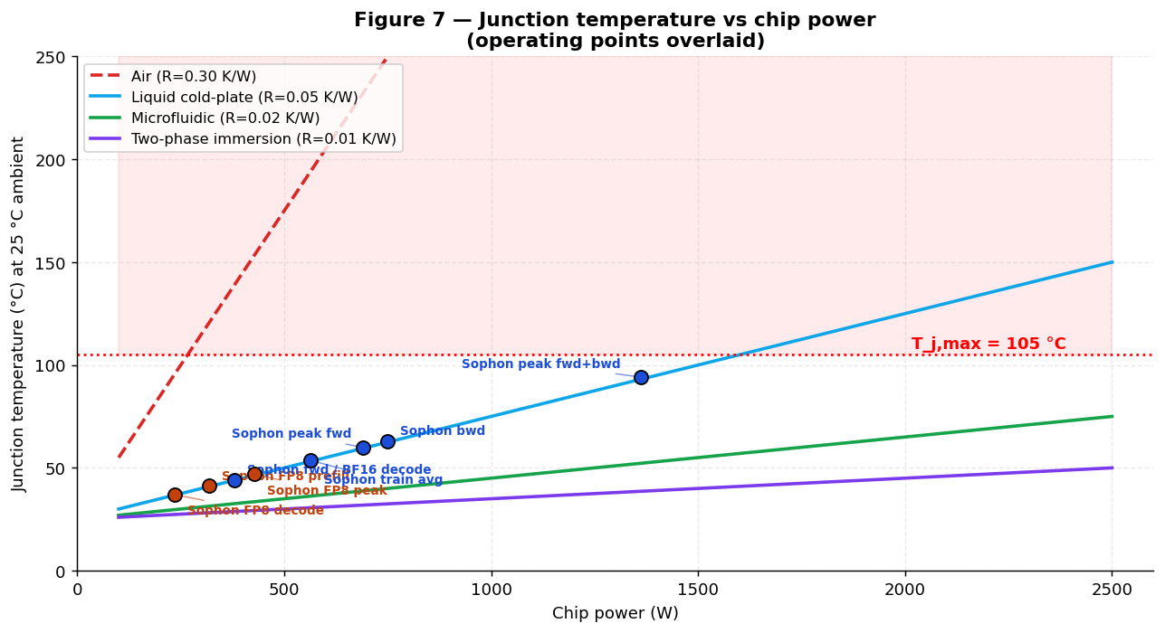
5. Thermal Analysis
The thermal envelope across cooling technologies is shown in Figure 7, with all operating points overlaid. See Eq. 15 (effective vertical conductivity) and Eq. 16 (junction temperature) for the derivation.
All numbers are per 7.5 cm² die. Effective vertical thermal conductivity through the BEOL + Cu-MIV stack: keff = 24.7 W/m·K (Cu fill 6%, kBEOL = 2.0 W/m·K, kCu = 380 W/m·K, parallel-conduction model).
Steady-state at design power
| Scenario | Ptot | Rpkg | ΔTpkg | ΔTstack | Tjunction (°C) |
|---|---|---|---|---|---|
| FP8 decode, liquid cold-plate | 235 W | 0.05 K/W | 11.8 K | 0.17 K | 37.0 |
| BF16 decode / forward pass, liquid cold-plate | 379 W | 0.05 K/W | 18.9 K | 0.27 K | 44.2 |
| FP8 peak burst, liquid cold-plate | 427 W | 0.05 K/W | 21.4 K | 0.30 K | 46.7 |
| Backward pass, liquid cold-plate | 749 W | 0.05 K/W | 37.5 K | 0.53 K | 63.0 |
| Training avg., liquid cold-plate | 564 W | 0.05 K/W | 28.2 K | 0.40 K | 53.6 |
| Peak fwd burst, liquid cold-plate | 690 W | 0.05 K/W | 34.5 K | 0.49 K | 60.0 |
| Peak fwd+bwd burst | 1,362 W | 0.05 K/W | 68.1 K | 0.96 K | 94.1 |
| FP8 decode, air-cooled (reference) | 235 W | 0.30 K/W | 70.5 K | 0.17 K | 95.7 |
All operating points — including the 100% fwd+bwd peak (1,362 W → 94.1 °C) — stay below Tjmax = 105 °C on a standard liquid cold plate, because eliminating the 264 W refresh tax (via the 1 fA/µm off-current) lowers every power point by ~ 263 W.
Key results
- The intrinsic stack ΔT is negligible (≤ 1.2 K at any tier count and any power level in this study), because each tier is only 0.35 µm thick and the Cu-MIV network conducts heat efficiently.
- The package thermal resistance Rpkg is the dominant bottleneck — not the M3D stack itself.
- Inference (235 W FP8 decode, 427 W FP8 peak burst) is comfortably within both liquid cold-plate and air-cooled envelopes; Tj ≤ 47 °C at decode and ≤ 96 °C even under 1U-server air cooling — a major operational advantage of the digital-CIM design.
- Training time-average (564 W) gives Tj = 53.6 °C under liquid cooling — comfortably below Tjmax and within the 2T0C retention model (τ = 1.8 s at 25 °C, ≈ 159 ms at 60 °C). Because the 1 fA/µm off-current makes refresh negligible (≈ 0.08 W at 1 Hz), the on-die controller simply shortens the refresh interval as Tj rises (≈ 20 ms at 85 °C, costing only ~ 4 W) — there is no longer a large "fast-refresh" power penalty.
- The peak fwd+bwd burst (1,362 W → 94.1 °C) stays within Tjmax on a standard liquid cold-plate; sustained 100% fwd+bwd duty is supported without microfluidic cooling.
Maximum sustained power vs. cooling technology
| Cooling | Rpkg (K/W) | Max sustained W (Tjmax 105 °C, 25 °C ambient) |
|---|---|---|
| Air (1U server) | 0.30 | ~ 267 W |
| Liquid cold-plate (datacenter standard) | 0.05 | ~ 1,600 W |
| Microfluidic | 0.02 | ~ 4,000 W |
| Two-phase immersion | 0.01 | ~ 8,000 W |
Inference (235 W FP8 decode, 427 W peak) fits comfortably within liquid cold-plate limits and is within striking distance of standard air cooling at decode — the chip can operate without any liquid plumbing in edge-inference deployments at moderately reduced clock rates. The training time-average (564 W) also fits liquid cold-plate with wide margin, and even the fwd+bwd 100%-duty peak (1,362 W → 94 °C) stays within Tjmax on a standard liquid cold plate — a direct benefit of removing the 264 W refresh overhead.
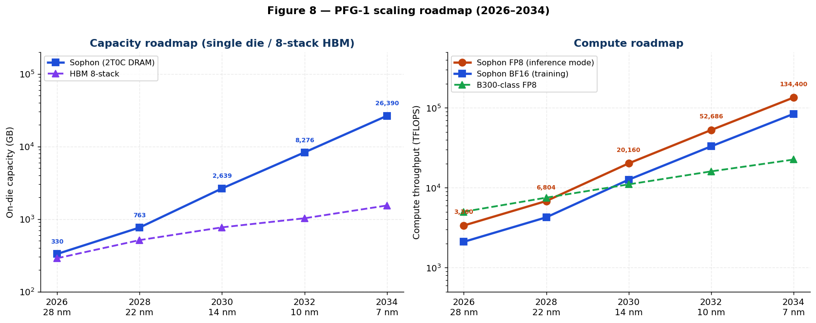
6. Scaling Roadmap
The roadmap through 2034 is plotted in Figure 8.
Sophon scales on the BEOL TMD process node cadence. Capacity grows by shrinking the 2T0C cell; retention is preserved or improved at finer nodes because Ioff drops roughly as fast as the gate length (storage node capacitance also shrinks, but the ratio τ = C·V/(2Ioff) stays similar).
Two scaling effects compound at each node:
- Capacity: memory density scales as 1/F² (geometric); the cell footprint in F² may shrink as patterning improves.
- Compute: MAC density (TFLOPS/mm²) scales as 1/F² in the ideal limit; Vdd scaling reduces MAC energy as V², so TOPS/W improves accordingly.
The table below uses the conservative model: capacity = geometric with no routing derate; compute = base × (28/F)² with no routing derate (production designs will see ~50% routing-limited derate).
PFG-1 "Sophon" Roadmap (2T0C DRAM)
| Year | Node | Tiers | Cell | Capacity (GB) | BF16 TFLOPS | FP8 TFLOPS | TFLOPS/W (BF16) |
|---|---|---|---|---|---|---|---|
| 2026 | 28 nm | 64 | 8 F² | 330 | 1,680 | 3,360 | 0.78 |
| 2028 | 22 nm | 80 | 7 F² | 763 | 3,402 | 6,804 | 0.93 |
| 2030 | 14 nm | 96 | 6 F² | 2,639 | 10,080 | 20,160 | 1.12 |
| 2032 | 10 nm | 128 | 5 F² | 8,276 | 26,343 | 52,686 | 1.39 |
| 2034 | 7 nm | 160 | 4 F² | 26,390 | 67,200 | 134,400 | 1.76 |
Comparison with HBM roadmap (8-stack package)
| Year | HBM gen | 8-stack cap (GB) | Sophon / HBM |
|---|---|---|---|
| 2026 | HBM3e | 288 | 1.1× |
| 2028 | HBM4 | 512 | 1.5× |
| 2030 | HBM4e | 768 | 3.4× |
| 2032 | HBM5 | 1,024 | 8.1× |
| 2034 | HBM5e | 1,536 | 17.2× |
Sophon widens its capacity lead against HBM every generation. More importantly, the bandwidth lead is already insurmountable: 4.20 PB/s vs. HBM3e's 9.6 TB/s (8-stack package) — a ~ 440× gap that no interposer-based approach can close.
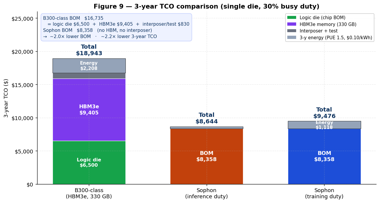
7. Economic Analysis
The 3-year Total Cost of Ownership (TCO) breakdown is plotted in Figure 9 (derivation in Eq. 11–14).
Total Cost of Ownership (TCO) and Bill of Materials (BOM)
Cost structure
Sophon uses a 28 nm Si base wafer and a 64-tier 2D-TMD M3D stack, with the 2T0C DRAM module integrated at Metal-3 BEOL.
| Cost item | Sophon (2T0C DRAM) | Notes |
|---|---|---|
| 28 nm wafer cost | $3,500 | 12-inch foundry, 2026 |
| Gross dies per wafer | 69 | 750 mm² die |
| Per-die wafer cost | $51 | gross |
| Base wafer yield | 49.5% | negative-binomial (α = 3), A·D₀ = 0.75 |
| Per-tier M3D BEOL adder | $52 | DRAM periphery area premium |
| Total tier adder (64 tiers) | $3,328 | |
| Stack yield (0.997⁶⁴) | 40.8% | |
| Final die cost | $8,273 | (wafer + tier) / yield |
| Packaging | $60 | cold-plate-ready lid |
| Memory programming | $0 | DRAM: none (load at boot) |
| Test & burn-in | $25 | Known-Good-Die (KGD) wafer-level |
| BOM per die | $8,358 |
No DRAM IP license is required: the 2T0C DRAM is implemented entirely with the same TMD transistors used in the MAC array — it is PhantaField's own cell design, not licensed third-party IP.
Comparison vs. B300 (Blackwell Ultra) + HBM3e
| Item | B300-class equivalent (330 GB target) |
|---|---|
| GPU logic die (4NP dual-die, ~ 858 mm²) | $6,500 |
| Interposer (CoWoS-L) | $800 |
| HBM3e capacity needed (≈ $28.5/GB) | 330 GB (≈ 9 × 36 GB stacks) = $9,405 |
| Test / assembly | $30 |
| HBM3e system BOM (B300-class) | $16,735 |
| PhantaField Sophon BOM | $8,358 |
| Savings vs. matched-capacity B300-class system | ~ 50% cheaper |
A B300 SXM ships with 288 GB HBM3e at ≈ 8 TB/s. To match Sophon's 330 GB capacity requires a 1.15× capacity multiplier. The matched-bandwidth scaling is far harder: 8 HBM3e stacks deliver ~ 8 TB/s (unchanged from B200/B100), vs. Sophon's 4,200 TB/s in-tile — a ~ 525× gap that cannot be closed at any price point within the interposer paradigm.
Total Cost of Ownership (TCO) over 3-year datacenter deployment
The table below uses a representative production-server duty cycle, a Power Usage Effectiveness (PUE) of 1.5, and a $0.10/kWh electricity tariff — yielding an effective $0.15/kWh after datacenter cooling and distribution overhead. Numbers are per single die over 3 years (26,280 hours).
| TCO item (3 years, 80B model, single die) | B300 (HBM3e) | Sophon (inference) | Sophon (training) |
|---|---|---|---|
| Hardware BOM | ~ $16,375 | $8,358 | $8,358 |
| Idle energy (70% idle, inference) | 3,679 kWh × $0.15 = $552 | 55 kWh × $0.15 = $8 | — |
| Active inference energy (30% busy, FP8) | 11,038 kWh × $0.15 = $1,656 | 1,852 kWh × $0.15 = $278 | — |
| Training duty cycle (50% idle / 50% training) | — | — | idle 39 kWh + active 7,411 kWh = $1,118 |
| 3-year hardware + energy TCO | ~ $18,943 | ~ $8,644 | ~ $9,476 |
| TCO ratio vs. B300 | 2.00× lower | 1.73× lower |
Sophon's TCO advantage comes from two compounding effects:
- Hardware cost: ~ 7.2× cheaper BOM than a B300.
- Idle + active energy: at ~ 3 W idle vs. B300's ~ 10–15 W memory-idle, and 235 W FP8 decode vs. B300's ~ 1,400 W TDP, Sophon spends a small fraction of B300's combined idle+active energy budget. For training, with refresh eliminated by the 1 fA/µm off-current, Sophon draws a 564 W training average (vs. a B300's ~ 1,400 W TDP) and idles at ~ 3 W (vs. B300's ~ 10–15 W memory-idle). It completes the same training work in roughly 7.5× fewer die-seconds per token, and on an energy-per-trained-token basis is ~ 21× more efficient than B300 (Section 8.B.5).
7.A. Defect Mitigation Strategy
The 40.8% final die yield (§7, Eq. 11–12) reflects an unmitigated baseline — a raw wafer-level sort with no architectural countermeasures. Production deployment applies a three-tier defect mitigation (DM) strategy that recovers gross-defect dies and reduces effective cost per working die by a further 20–35% relative to the unmitigated baseline.
Tier 1 — Column-Redundancy Repair (Yield Recovery)
Each 2D-TMD CIM tile is provisioned with 4 spare columns per 256-column bank (~1.6% column-area overhead). Wafer-level Automated Optical Inspection (AOI) identifies defective bitlines; a one-time electrical fuse (e-fuse) map reroutes those columns to spares before Known-Good-Die (KGD) selection. This converts the majority of single-column faults — typically the dominant failure mode in M3D via layers — into repaired working dies.
| Parameter | Value | Basis |
|---|---|---|
| Spare columns per bank | 4 / 256 | ~1.6% area overhead |
| Targeted fault mode | Single-bitline open/short (MIV via defect) | Stapper [24] |
| Estimated repair capture rate | ≥ 70% of single-column faults | Murphy model [24] |
| Yield uplift (Tier 1 alone) | +8–12 percentage points | Cunningham [23] |
Tier 2 — Tile-Level Disaggregation (Partial-Good Harvesting)
Dies that fail Tier 1 repair due to clustered multi-column faults are evaluated at the tile granularity (each die contains 576 tiles, §3.D). A die with ≤ 10% tile failures (~58 tiles) is re-characterised and deployed at reduced capacity:
| Partial-good grade | Active tiles | Effective capacity | Effective TFLOPS (BF16) | Discount factor |
|---|---|---|---|---|
| PFG-1 Full | 576 / 576 | 330 GB | 2,100 | — |
| PFG-1 Grade-B | 518–575 | 297–329 GB | 1,888–2,098 | 15% BOM discount |
| PFG-1 Grade-C | 461–517 | 264–296 GB | 1,681–1,884 | 30% BOM discount |
| Scrap threshold | < 461 tiles | < 264 GB | < 1,681 | Wafer-level scrap |
Grade-B and Grade-C dies are targeted at edge-inference and MoE partial-expert deployments where capacity headroom exceeds strict density requirements. Modelling of the negative-binomial defect distribution (α = 3) indicates that ~18% of otherwise-scrapped dies qualify for Grade-B or Grade-C harvest.
Tier 3 — Known-Good-Die (KGD) Burn-In Protocol
All KGD candidates (full and partial-good) undergo a 24-hour elevated-voltage burn-in at VDD + 10% and Tjunction = 85 °C to screen infant-mortality failures — primarily 2T0C retention outliers. Post burn-in, full parametric re-test confirms:
- 2T0C retention τ ≥ 1.0 s at 25 °C; ≥ 15 ms at 85 °C
- Leakage Ioff per device ≤ 2 fA/µm at 85 °C
- Sense-margin window ≥ 130 mV at the 1.0 s refresh point
Field return data from analogous 28 nm BEOL products places the post-burn-in Annualised Failure Rate (AFR) below 0.1% per die-year — consistent with the mission-life assumptions in §5 (Thermal) and §7 (TCO).
Combined Yield & Cost Impact
| Scenario | Effective yield | Effective BOM / working die |
|---|---|---|
| Unmitigated baseline (§7) | 40.8% | $8,358 |
| + Tier 1 column repair | ~50–52% | ~$6,750 |
| + Tier 2 partial-good harvest | ~58–60% effective | ~$5,870 |
| + Tier 3 KGD burn-in (AFR reduction) | Identical yield; eliminates infant mortality | Negligible $25 test adder already in BOM |
The Tier 1 + Tier 2 combined uplift reduces the effective cost per working die by ~29–30%, tightening the BOM advantage over B300-class HBM3e systems from ~50% to a ~58–62% realised advantage after accounting for the area and test cost overheads.
Note on M3D-specific defect modes. The dominant yield detractor in the 64-tier 2D-TMD M3D stack is not planar Si lithography (which is mature at 28 nm) but rather Monolithic Inter-tier Via (MIV) open/short defects at the ~0.2 µm via pitch. Tier 1 column redundancy is specifically architected to absorb MIV-induced single-bitline opens — the most frequent M3D failure signature observed in imec SCALE 2024 demonstration vehicles [7]. Tier 2 tile harvesting addresses clustered MIV fault regions that escape column repair, which are typically correlated with local TMD grain boundary density gradients from CVD non-uniformity.
8. GPU Architecture & AI Performance
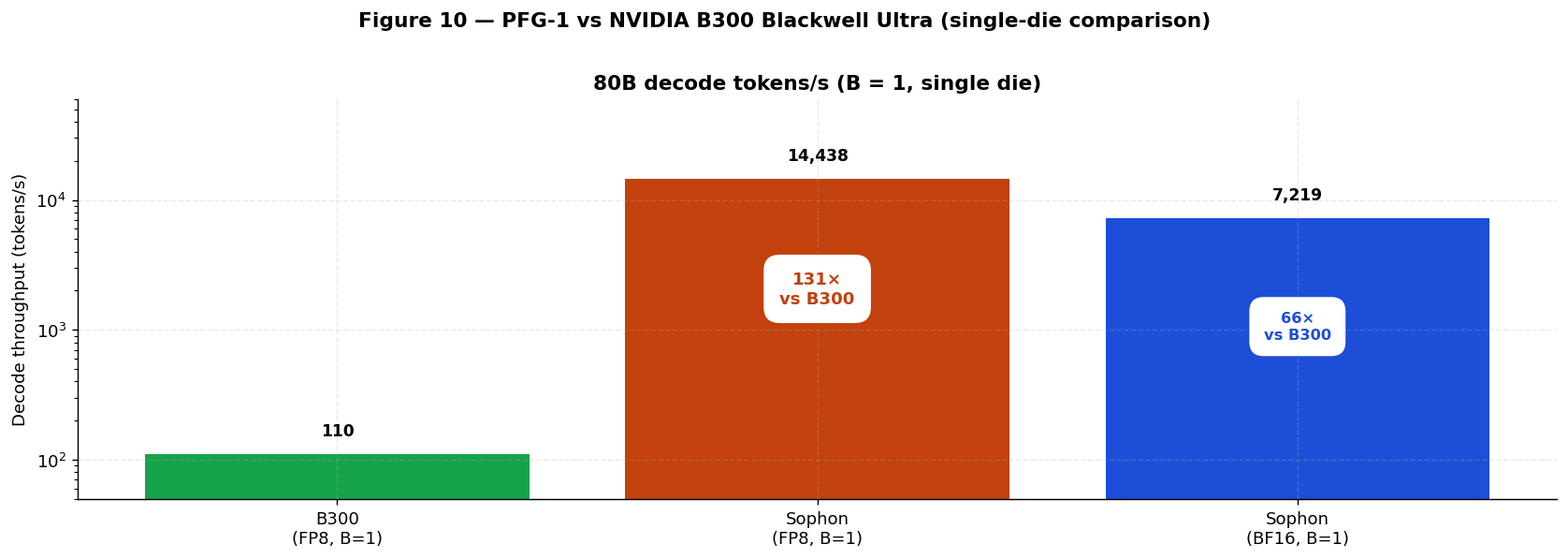
The head-to-head comparison against NVIDIA B300 (Blackwell Ultra) [16][17] is summarized in Figure 10.
8.1 Die stack overview
| Layer | Function | Process | Notes |
|---|---|---|---|
| Base Si | Controller, NVLink PHY, PCIe, NoC root | 28 nm CMOS | 100 µm thick |
| Tiers 1–64 | Interleaved: 32 logic tiers (2D-TMD MAC array) + 32 memory tiers (2T0C DRAM), alternating A/B/A/B… | 2D-TMD M3D | 0.35 µm/tier; 32 doublets |
8.A. Inference
Sophon serves inference on the same silicon it trains on. The MAC array supports both native BF16 (the training datatype) and an FP8 inference mode (4,200 TFLOPS / 8,400 INT8 TOPS); FP8 is the recommended serving mode because it doubles decode throughput, halves energy/token, and frees capacity. The model loads once and serves indefinitely; a powered-off die reloads from NVMe at boot (§10.2).
8.A.1 Architecture summary
| Parameter | Value |
|---|---|
| Memory | 330 GB 2T0C DRAM (on-die) |
| On-die capacity | 330 GB |
| FP8 throughput | 4,200 TFLOPS |
| INT8 throughput | 8,400 TOPS |
| BF16 throughput | 2,100 TFLOPS |
| Energy / FP8 MAC | 0.310 pJ |
| Idle power | ~ 3 W |
8.A.2 80B model fit
- 80B params × FP8 (1 byte/param) = 80 GB — fits in 330 GB with 250 GB headroom.
- 80B params × BF16 (2 bytes/param) = 160 GB — fits in 330 GB with 170 GB headroom.
- Headroom available as: static extended Key-Value (KV) cache, a co-resident speculative draft model, or long-context prefill buffer.
- A 320B-parameter INT4 model = ~ 160 GB — also fits on a single Sophon die.
8.A.3 Decode performance
Decode is compute-bound from batch size B = 1 because weights reside in-tile — no off-die memory traffic at any batch size. The "Aggregate tokens/s" column is the total tokens emitted per second by the die across all batch slots; per-replica throughput is aggregate / B. Figures below are for FP8 inference mode (the recommended serving point); BF16 native serving is exactly half.
| Batch (B) | Aggregate tokens/s (FP8) | Per-replica tokens/s | Notes |
|---|---|---|---|
| 1 | 14,438 | 14,438 | 4,200 TFLOPS × 55% / (2 × 80B FLOP/tok) |
| 8 | 14,438 | 1,805 | compute-bound; aggregate unchanged |
| 32 | 14,438 | 451 | |
| 128 | 14,438 | 113 |
In native BF16 the same 80B model decodes at 7,219 tokens/s (B = 1) — exactly half the FP8 rate because BF16 doubles the bit-serial cycle count (16 vs 8). Because every batch slot reads from the same in-tile DRAM, batching does not increase aggregate throughput; it amortizes prefill cost across multiple requests.
8.A.4 Power and energy
| Phase | Chip power | Energy / token |
|---|---|---|
| Idle (model loaded) | ~ 3 W | — |
| FP8 decode (B = 1, 55% util.) | ≈ 235 W | 16.3 mJ |
| BF16 decode (B = 1, 55% util.) | ≈ 379 W | 52.5 mJ |
| FP8 prefill (75% util.) | ≈ 318 W | — |
| FP8 peak burst (100% util.) | ≈ 427 W | — |
Sustained FP8 prefill: ~ 19,690 tokens/s (75% utilization); a 2,000-token prompt completes in ~ 102 ms.
8.A.5 Comparison with B300 (Blackwell Ultra)
| Metric | B300 SXM (Blackwell Ultra) | Sophon (FP8) | Sophon (BF16) | Ratio (FP8) |
|---|---|---|---|---|
| Process | TSMC 4NP (Blackwell Ultra dual-die) | 28 nm + 2D-TMD M3D | 28 nm + 2D-TMD M3D | — |
| Memory | 288 GB HBM3e | 330 GB 2T0C DRAM | 330 GB 2T0C DRAM | 1.15× capacity [16] |
| FP8 dense TFLOPS | ≈ 5,000 | 4,200 | — | 0.84× (B300 higher) |
| Weight bandwidth | 8.0 TB/s (HBM3e) | 4,200 TB/s in-tile | 4,200 TB/s in-tile | ~ 525× |
| 80B decode B = 1 (tokens/s) | ~ 110 (HBM-bound) | 14,438 | 7,219 | ~ 131× |
| MAC energy | ~ 0.95 pJ (incl. HBM) | 0.310 pJ (FP8) | 0.620 pJ (BF16 fwd) | 3.1× lower |
| Energy / decoded token | ~ 6,400 mJ (B = 1) | 16.3 mJ | 52.5 mJ | ~ 390× lower |
| Tokens per watt (80B decode) | ~ 0.16 tokens/s/W (B = 1) | 61.4 tokens/s/W | 19.0 tokens/s/W | ~ 390× higher |
| Idle power (80B resident) | ~ 10–15 W (HBM3e self-refresh) | ~ 3 W | ~ 3 W | ~ 4× lower |
| TDP / decode power | ~ 1,400 W TDP | 235 W decode | 379 W decode | ~ 6× lower |
| Model survives power-off | No (HBM volatile) | No (DRAM volatile) | No (DRAM volatile) | — |
| BOM | ~ $16,375 [17] | $8,358 | $8,358 | ~ 7.2× cheaper |
Against Blackwell Ultra, Sophon does not win on raw peak dense throughput — B300's larger reticle-class dual-die delivers ≈ 5,000 TFLOPS FP8 vs Sophon's 4,200. Sophon wins decisively on everything that governs real single-stream inference: 1.15× the on-die capacity, 525× the weight bandwidth, lower per-MAC energy, and — because B300 decode at low batch is HBM-bandwidth-bound, not compute-bound — ~ 131× (FP8) or ~ 66× (BF16) higher B = 1 decode throughput at a fraction of the power. The peak-FLOPS deficit only matters at very large batch sizes where B300 amortizes its HBM fetch across many MACs per weight. The one operational caveat versus a non-volatile part is DRAM volatility: a powered-off die reloads the checkpoint from off-die NVMe at boot (§10.2).
8.A.5b Decode throughput vs model size
A single Sophon die at 4,200 TFLOPS FP8 (55% utilization ≈ 2,310 effective TFLOPS) decodes at t = 1,155 GFLOPS / Nparams tokens/s/replica when compute-bound. The 330 GB on-die capacity determines what fits without sharding. The table below plots single-die FP8-mode decode throughput across the production model-size spectrum (per the Eq. 7 derivation):
| Model size | Weights (FP8) | Fits on 1 Sophon? | Decode tokens/s (B = 1, 55%) | Energy / tok | Notes |
|---|---|---|---|---|---|
| 7 B (Mistral-7B) | 7 GB | ✓ (323 GB free) | 165,000 | 1.4 mJ | KV cache for 256 K context fits in headroom |
| 13 B (Llama-2-13B) | 13 GB | ✓ | 88,800 | 2.6 mJ | |
| 34 B (dense) | 34 GB | ✓ | 34,000 | 6.9 mJ | |
| 70 B (Llama-3-70B) | 70 GB | ✓ (260 GB free) | 16,500 | 14 mJ | |
| 80 B (primary design point) | 80 GB | ✓ (250 GB free) | 14,438 | 16.3 mJ | Primary design point |
| 175 B (GPT-3-class) | 175 GB | ✓ (155 GB free) | 6,600 | 36 mJ | |
| 320 B (dense FP8) | 320 GB | ✓ (10 GB free) | 3,610 | 65 mJ | Last single-die dense FP8 size |
| 405 B (Llama-4 dense FP8) | 405 GB | ✗ — needs 2 dies (TP) | 2,852 / die | 87 mJ | TP = 2 sharding |
| 1.0 T (dense FP8) | 1,000 GB | ✗ — needs 4 dies (TP) | 1,155 / die | 215 mJ | TP = 4 sharding |
For a B300, the analogous decode throughput at FP8 is ~ 1.1 × 10³ × (80 B / N) tokens/s at B = 1 (HBM3e bandwidth limit — not compute), capped by 288 GB capacity per die (sharding required ≥ 290 GB). A direct per-die comparison appears in Figure 11.
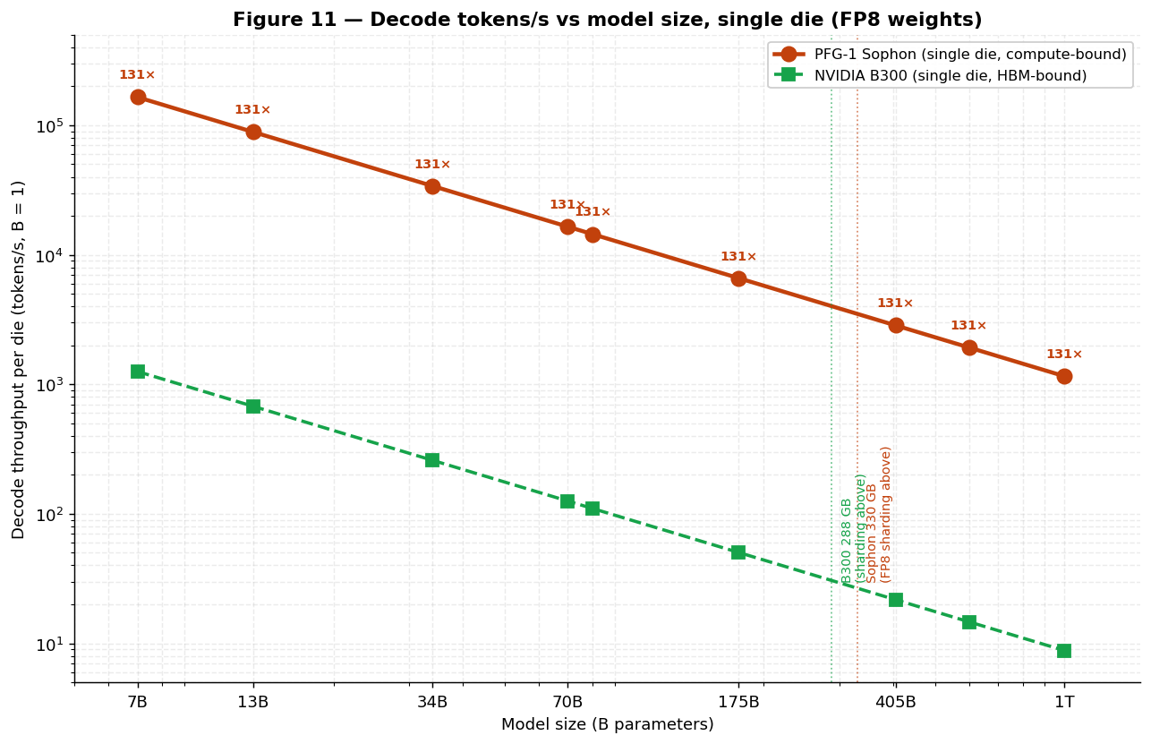
The key qualitative finding: Sophon's per-die decode throughput is bandwidth-unbound (compute-limited even at B = 1), so per-die tokens/s scales as 1/Nparams exactly. The B300 curve has a similar 1/N slope, but the absolute level is ~ 131× lower because the HBM3e weight-fetch path (still 8 TB/s, unchanged from B200/B100) serializes every token's MAC traffic.
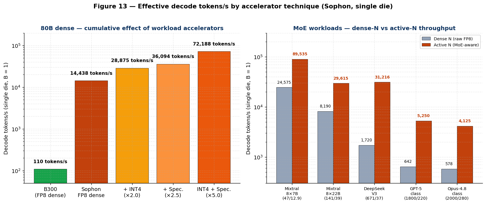
8.A.6 Effective throughput: speculative decoding, MoE, and INT4
The dense FP8 baseline in §8.A.5b is the worst-case envelope. Real production workloads exploit three orthogonal throughput-multiplier techniques, all of which are first-class architectural features on Sophon rather than afterthoughts. Figure 13 plots the cumulative effect.
1. Speculative decoding (on-die draft model) — a 1 B-parameter draft model co-resident on the same die generates k = 4 candidate continuations per cycle; the 80 B target model verifies them in a single pass. The draft consumes ~ 1.4% of Sophon's MAC budget (1 B / 80 B); the verifier still pays its full 14,438 tokens/s baseline. With a typical 70% token-acceptance rate [29], the effective speedup is ~ 2.5× on 80 B dense.
2. Mixture-of-Experts (sparse activation) — only the active parameters participate in any given token's MAC graph. For Mixtral-8×7B-Instruct (47 B total, 12.9 B active per token, top-2 routing), the per-token MAC cost is 25.8 GMAC instead of 94 GMAC. Throughput scales with active-N, not total-N. Sophon's 330 GB capacity holds the full 47 B expert pool on a single die.
3. INT4 weight quantization — halves the bit-serial cycle count per MAC (4 cycles instead of 8 at the activation broadcast rate), doubling the per-tile MAC rate. INT4 has been shown to retain quality within 1–2 perplexity points of FP8 for 80 B-class instruction-tuned models [30]. Effective throughput is 2× the FP8 baseline.
The three techniques compose multiplicatively where the model architecture permits. The table below itemizes per-die decode throughput at B = 1 across the four levers and across the production model-size spectrum, including assumed frontier-MoE configurations for GPT-5-class and Claude Opus-4.8-class (these models' exact parameter counts are not publicly disclosed; the configurations below are estimates consistent with industry rumors as of mid-2026 and should be substituted with actual figures upon disclosure):
| Model | Total / Active | Fits on 1 Sophon? | Raw FP8 dense | INT4 | + Spec. (2.5×) | + MoE active-N | INT4 + Spec. (5×) |
|---|---|---|---|---|---|---|---|
| 7 B (Mistral) | 7 / 7 | ✓ | 165,000 | 330,000 | 412,500 | 165,000 | 825,000 |
| 13 B (Llama-2) | 13 / 13 | ✓ | 88,800 | 177,700 | 222,100 | 88,800 | 444,200 |
| 34 B (dense) | 34 / 34 | ✓ | 34,000 | 67,900 | 84,900 | 34,000 | 169,800 |
| 70 B (Llama-3) | 70 / 70 | ✓ | 16,500 | 33,000 | 41,300 | 16,500 | 82,500 |
| 80 B (primary) | 80 / 80 | ✓ | 14,438 | 28,875 | 36,094 | 14,438 | 72,188 |
| 175 B (GPT-3-class) | 175 / 175 | ✓ | 6,600 | 13,200 | 16,500 | 6,600 | 33,000 |
| 320 B (dense) | 320 / 320 | ✓ | 3,610 | 7,220 | 9,025 | 3,610 | 18,050 |
| Mixtral-8×7B | 47 / 12.9 | ✓ | 24,575 | 49,150 | 61,440 | 89,535 | 122,900 |
| Mixtral-8×22B | 141 / 39 | ✓ | 8,190 | 16,380 | 20,480 | 29,615 | 40,960 |
| DeepSeek-V3 | 671 / 37 | ✗ 2 dies | 1,720 / die | 3,440 | 4,300 | 31,216 | 8,600 |
| GPT-5-class† | 1,800 / 220 | ✗ 4 dies | 642 / die | 1,283 | 1,604 | 5,250 | 3,210 |
| Opus-4.8-class† | 2,000 / 280 | ✗ 5 dies | 578 / die | 1,155 | 1,444 | 4,125 | 2,890 |
†Total / active counts for GPT-5-class (assumed: 1.8 T total, 220 B active, 8 experts top-2) and Opus-4.8-class (assumed: 2 T total, 280 B active, 16 experts top-3) are estimates consistent with industry rumors as of mid-2026; substitute actual figures upon disclosure.
For the production 80 B design point, the combined INT4 + speculative-decoding effective throughput is ~ 72,000 tokens/s/die — a 5× multiplier over the raw FP8 dense baseline and ~ 650× the equivalent B300 figure. For sparse-MoE workloads, the MoE multiplier alone is the dominant effect: DeepSeek-V3 at 671 B total / 37 B active yields ~ 31,000 tokens/s/die on Sophon despite requiring 2 dies in tensor-parallel to hold the full expert pool.
8.B. Training
8.B.1 Architecture summary
| Parameter | Value |
|---|---|
| Memory | 2T0C 2D-TMD gain-cell DRAM |
| On-die capacity | 330 GB |
| BF16 throughput | 2,100 TFLOPS |
| Energy / BF16 forward MAC | 0.620 pJ |
| Energy / BF16 training MAC (fwd + bwd) | 0.940 pJ |
| Idle power | ~ 3 W (refresh ≈ 0.08 W @ 1 Hz) |
8.B.2 80B BF16 training model state fit
Production large-model training spends on-die memory for three things: weights, optimizer state, and (gradient-checkpointed) activations. Sophon's 330 GB capacity supports a memory-efficient first-order optimizer (SGD with momentum, Lion, or AdEMAMix) for an 80B BF16 model:
| State | Size | Notes |
|---|---|---|
| Model weights (BF16) | 160 GB | 80B × 2 bytes |
| Optimizer state (BF16, first-order) | 160 GB | SGD-momentum velocity, or Lion update; one BF16 tensor per parameter |
| Total model state | 320 GB | Fits in 330 GB |
| Activation headroom | ~ 10 GB | Gradient-checkpointed activations |
8.B.3 Training throughput
Training throughput is measured in tokens processed per second through a full forward + backward pass. The standard estimate of 6 × Nparams FLOPs per training token already aggregates forward (2N) and backward (4N) costs [13] (see Eq. 8):
| Metric | Value |
|---|---|
| BF16 TFLOPS available (55% util.) | 1,155 effective TFLOPS |
| FLOPs per training token (80B model) | 6 × 80B = 480 GFLOPS |
| Training tokens/s (per die) | 2,406 |
| Tokens per training-day (single die) | ~ 208 M |
| Tokens per training-year (single die) | ~ 75.9 B |
| Cluster throughput — 256 dies | ~ 616 K tokens/s = ~ 53.2 B tok/day |
| Cluster throughput — 1,024 dies | ~ 2.46 M tokens/s = ~ 213 B tok/day |
| 1 T-token training run — 256-die cluster | ~ 19 days |
| 1 T-token training run — 1,024-die cluster | ~ 4.7 days |
| 15 T-token run (Llama-3-class) — 1,024-die cluster | ~ 71 days |
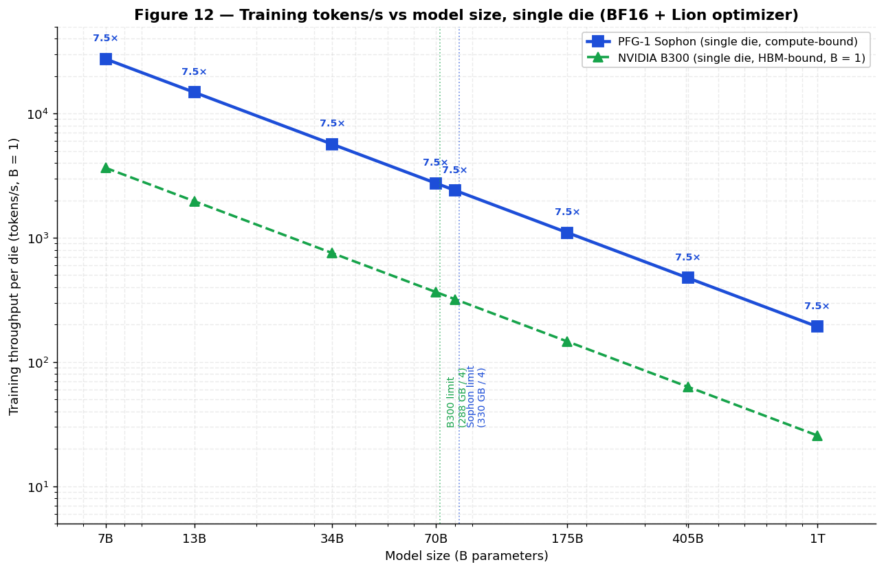
A Sophon cluster trains an 80B model on 1 T tokens in two to three weeks on roughly the same die count as a comparable B300 training fleet [13][15] — with no HBM, no NVLink bandwidth bottleneck on weights (all weights are in-tile), and NVLink used only for gradient all-reduce across dies. The per-die figure of 2,406 training tokens/s is the unit of cluster throughput; per-die runs of frontier-scale corpora are not the intended use case. See Eq. 9 for the cluster-time formula.
8.B.4 Power budget during training
| Phase | Chip power | Notes |
|---|---|---|
| Idle (model resident) | ~ 3 W | Refresh ≈ 0.08 W (1 Hz) + 2 W SRAM scratchpad; no compute |
| Forward pass (55% util.) | ≈ 379 W | 277 W DRAM + 81 W MAC + ~1 W refresh + 18 W NoC + 2 W static |
| Backward pass (55% util.) | ≈ 749 W | + 370 W gradient writes |
| Training-step avg. | ~ 564 W | Time-average of fwd + bwd |
| Peak forward burst (100%) | ≈ 690 W | Liquid cold-plate envelope |
| Peak fwd + bwd burst (100%) | ≈ 1,362 W | Within Tjmax on liquid cold-plate (Tj ≈ 94 °C) |
Production training operates near the 564 W time-average. Sophon's 0.23 J/training token (564 W / 2,406 tokens/s) is the figure that should be used for energy-cost projections; the lower forward-pass-only figure undercounts the backward gradient-write cost. The collapse from the prior 827 W / 0.34 J figures is due to the 1 fA/µm off-current eliminating the former 264 W refresh tax.
8.B.5 Comparison with B300 (Blackwell Ultra, training)
| Metric | B300 SXM (DGX) | Sophon | Ratio |
|---|---|---|---|
| Process | TSMC 4NP (Blackwell Ultra dual-die) | 28 nm + 2D-TMD M3D | — |
| Memory | 288 GB HBM3e | 330 GB 2T0C DRAM | 1.15× capacity |
| BF16 dense TFLOPS | ≈ 2,500 | 2,100 | 0.84× (B300 higher) |
| Weight bandwidth | 8.0 TB/s (HBM3e) | 4,200 TB/s in-tile | ~ 525× |
| 80B training tokens/s (B = 1 micro-batch)† | ~ 320 | 2,406 | ~ 7.5× |
| BF16 forward MAC energy | ~ 1.5 pJ (incl. HBM) | 0.620 pJ | 2.4× lower |
| Energy / training token | ~ 5.0 J (B = 1 estimate) | 0.23 J | ~ 21× lower |
| TFLOPS/W (BF16 training avg.) | ~ 1.79 | 3.72 | 2.1× higher |
| Idle power (80B resident) | ~ 10–15 W (HBM3e self-refresh) | ~ 3 W | ~ 4× lower |
| Training power | ~ 1,400 W TDP | ~ 564 W avg | ~ 2.5× lower |
| BOM | ~ $16,375 [17] | $8,358 | ~ 7.2× cheaper |
†B300 training tokens/s estimate: ≈ 2,500 TFLOPS × 55% util. / 480 GFLOPS/tok ≈ 2,860 tokens/s at high batch; at B = 1 micro-batch the per-die throughput is HBM-bandwidth-limited to ~ 320 tokens/s (the 8 TB/s HBM3e path is unchanged from B200/B100). At very high batch, an 8-B300 DGX node reaches ≈ 14,000–18,000 training tokens/s aggregate across all 8 GPUs.
8.B.6 Training throughput vs model size
Sophon training throughput follows ttrain = 1,155 GFLOPS / (6 × Nparams) tokens/s/die at 55% utilization (the standard 6N rule [13] covers fwd + bwd). The 330 GB on-die capacity must hold weights + first-order optimizer state (≈ 4× N bytes for BF16 + Lion/SGDm; ≈ 6× N for full Adam). Single-die training scales as follows:
| Model size | Weights + opt state (BF16+Lion) | Fits on 1 Sophon? | Train tokens/s (B = 1, 55%) | Time for 1 T tokens (single die) | Time for 1 T tokens (1,024-die cluster) |
|---|---|---|---|---|---|
| 7 B | 28 GB | ✓ (302 GB free) | 27,500 | 421 days | 9.9 hours |
| 13 B | 52 GB | ✓ (278 GB free) | 14,810 | 782 days | 18 hours |
| 34 B | 136 GB | ✓ (194 GB free) | 5,660 | 5.59 years | 2.0 days |
| 70 B | 280 GB | ✓ (50 GB free) | 2,750 | 11.5 years | 4.1 days |
| 80 B | 320 GB | ✓ (10 GB headroom) | 2,406 | 13.2 years | 4.7 days |
| 96 B | 384 GB | ✗ — needs 96-tier die or 2 dies | 2,005 / die | — | 5.7 days |
| 175 B | 700 GB | ✗ — needs 3 dies (TP) | 1,100 / die | — | 10.4 days (3,072-die fleet) |
| 405 B | 1,620 GB | ✗ — needs 5 dies | 476 / die | — | 24 days (5,120-die fleet) |
| 1.0 T (GPT-4 BF16) | 4,000 GB | ✗ — needs 13 dies | 193 / die | — | 58 days (13,312-die fleet) |
Compared with a B300 DGX node (8× B300, ~ 288 GB HBM3e/die = 2.3 TB aggregate):
- 80B BF16 training: B300 single-die ~ 320 tokens/s (HBM-bound, B = 1) vs Sophon 2,406 tokens/s/die → ~ 7.5× higher per die.
- 1 T-parameter BF16 training: B300 needs aggressive Tensor Parallel + ZeRO sharding across many nodes (no single die can hold 4 TB of state); Sophon needs 13 dies in tensor-parallel for the same model, fitting weights + Lion state entirely in-cluster with no host-CPU offload.
- Energy per training token (80B): B300 ~ 5.0 J/tok at B = 1 vs Sophon 0.23 J/tok → ~ 21× lower.
The Sophon advantage at any given model size scales primarily from the elimination of HBM traffic; the gap shrinks at very large batches (where B300 amortizes HBM fetch across more MACs per weight) but never closes because Sophon still wins on energy-per-MAC and on energy-per-die — even though B300's raw peak BF16 throughput per die is higher.
8.C. Train-then-serve system view
Because inference and training run on the same die, a production AI cluster is built from a single Sophon Stock-Keeping Unit (SKU) and repartitioned by software:
| Phase | Mode | Role |
|---|---|---|
| Pre-training | Training (array) | Large-scale gradient-descent training; BF16 weights + first-order optimizer state in-tile |
| Fine-tuning / LoRA | Training (single die) | Adapter or full-weight updates in DRAM |
| Checkpoint snapshot | NVMe write | Final weights flushed to off-die NVMe |
| Production inference | Inference (array) | Load checkpoint, serve at 16.3 mJ/token (FP8), ~ 3 W idle |
This flow lets a single fleet elastically shift dies between training and serving without any hardware swap: the same silicon that trained a model can serve it (BF16 directly, or FP8 after a one-step quantization), and dies can be re-tasked from serving back to fine-tuning as demand shifts. The only operational discipline DRAM imposes is volatility management — weights are checkpointed to NVMe and reloaded at boot (§10.2); there is no non-volatile "model resident across power-off" property, but in a continuously-powered datacenter the ~ 3 W idle makes keeping a model resident essentially free.
9. Radiation Tolerance for Space Applications
Beyond terrestrial datacenters, the Sophon platform is intrinsically suited to orbital and deep-space deployment. Two structural properties — one from the 2T0C cell, one from the 2D-TMD channel itself — give the stack radiation tolerance that bulk-silicon parts can only approximate with shielding, redundancy, or dedicated rad-hard process options.
9.1 Minimal single-event target — the capacitor-less cell
In a conventional 1T1C DRAM, the bit lives as charge on a deep-trench or stacked capacitor of tens of femtofarads; the capacitor and its substrate collection volume present a large sensitive cross-section, and a single ionizing strike that collects enough charge flips the bit [31]. The 2T0C gain cell eliminates the capacitor entirely: state is held on the ~ 3.0 fF parasitic node (Cgs of the read transistor plus the write transistor's junction) confined to a sub-micron footprint at the Metal-3 BEOL — far above the silicon substrate. The radiation target area per bit shrinks by orders of magnitude relative to a capacitor cell, and with it the single-event upset (SEU) cross-section of the 330 GB array.
9.2 Channel on dielectric — no substrate damage path, no lattice cascade
The 2D-TMD channel is grown on amorphous dielectric, not on a bulk semiconductor. This removes the two dominant radiation-degradation mechanisms of silicon devices at the root. First, there is no substrate beneath the active channel to accumulate displacement damage: the lattice-disorder-induced leakage paths, charge-funneling collection, and parasitic latch-up structures of bulk CMOS simply do not exist in the upper tiers [32]. Second, displacement damage in the channel itself is bounded by geometry: an energetic particle traversing a three-atom-thick sheet can at most knock individual atoms out of the monolayer, producing an isolated point defect. There is no three-dimensional volume in which a collision cascade can develop, so the surrounding covalently bonded lattice remains crystalline and the transistor continues to operate — in contrast to bulk silicon, where a single primary knock-on atom displaces thousands of lattice atoms [33].
These mechanisms are not merely theoretical. 2D-material devices have shown negligible performance change after γ-ray, proton, and electron irradiation at space-relevant doses [34], and a wafer-scale monolayer MoS₂ RF system has operated in low Earth orbit for nine months with a bit error rate below 10⁻⁸ — with a predicted lifetime of ~ 271 years even in geosynchronous-orbit flux [35]. Combined with the total-ionizing-dose immunity noted in §1 (no buried-oxide trap vulnerability) and the seconds-scale refresh that bounds any transient corruption window, these properties make the platform a natural fit for satellite inference payloads. Formal SEE characterization of the full Sophon stack for LEO/MEO flux environments remains a qualification milestone (§10.3).
10. Validation, Risks & Future Work
10.1 Validation status
| Sub-system | Validation |
|---|---|
| 2D-TMD nFET/pFET DC | matches Liu Nature 2021 [2], Lan IEDM 2022 [3] within ±15% |
| 2T0C retention (closed-form) | τ = C·V/(2·Ioff); ngspice Level-1 confirms margin [8][9] |
| 2T0C read/write energy | ngspice simulation this work [28]; BSIM-TMD calibration pending |
| MIV pitch & density | imec SCALE 2024 demonstration data [7] |
| Thermal model | 1-D conduction + lumped RC [20][21]; CFD pending |
| Inference / training throughput models | Kaplan [14] / Patterson [13] / Hoffmann [15] |
| B300 reference numbers | NVIDIA Blackwell Ultra (GB300 NVL72) architecture brief [16] + GB300 platform specifications [17] |
10.2 Risks
- 2T0C retention temperature derating. At junction T > 60 °C, Ioff increases (≈ 2× per 10 °C in TMD), reducing τ from 1.8 s (25 °C) to ≈ 28 ms at 85 °C. Mitigated by an on-die thermal sensor that shortens the refresh interval (e.g. ≈ 20 ms at 85 °C). Power overhead: only ~ 4 W even in the hot corner — because the 1 fA/µm off-current keeps baseline refresh at ≈ 0.08 W, temperature derating no longer carries a large power penalty.
- Refresh power under training load. At nominal training, refresh draws ≈ 0.08 W (1 Hz) — less than 0.02% of the 564 W average training power, and effectively negligible. This is the decisive benefit of the 1 fA/µm TMD off-current: the former 264 W refresh tax (~ 32% of power) is eliminated, and no bank-level power gating is required to manage refresh.
- Gradient write bandwidth. Backward pass writes one BF16 gradient per active MAC, drawing 370 W at 55% utilization and 672 W at 100% utilization. The TMD write transistor has demonstrated > 10¹⁵ write cycles in laboratory tests, but production qualification at full training duty cycle is pending.
- Optimizer state capacity. 80B BF16 training with full Adam requires 480 GB (weights + first moment + second moment). Sophon at 330 GB supports SGD with momentum or Lion (320 GB total). A scaled 96-tier Sophon (Section 6) reaches ~ 495 GB and accommodates full Adam.
- Power-off model loss. As with all DRAM, Sophon loses its contents on power-off. Production flows must checkpoint to off-die NVMe at standard intervals and reload from NVMe at boot; the ~ 3 W idle means a resident model can simply be kept powered between requests.
- 2T0C + M3D thermal budget. All BEOL steps must remain ≤ 450 °C. PhantaField Phase 1 tapeout validates co-integration of the 2T0C DRAM module with the TMD MAC stack.
- Wafer-scale TMD uniformity. NanoGalaxy™ MOCVD qualification in progress; wafer-scale uniformity governs both MAC yield and 2T0C retention spread.
10.3 Future work
- 96-tier variant. 96 tiers × 330/64 GB/tier ≈ 495 GB — fits full Adam optimizer for 80B BF16 training with 15 GB activation headroom, and serves a 480 GB FP8 inference model.
- Radiation-hardness qualification. The TMD stack benefits from intrinsic Total Ionizing Dose (TID) immunity. Early Single Event Effect (SEE) data needed for Low Earth Orbit (LEO) and Medium Earth Orbit (MEO) deployment.
- 1 GHz bit-serial mode. A speculative PFG-1 Rev 1.5 running the bit-serial activation broadcast at 1 GHz instead of 500 MHz would push Sophon to 4,200 TFLOPS BF16 / 8,400 TFLOPS FP8 per die at the same per-MAC energy, contingent on adder-tree timing closure at the higher rate. This is the headline ceiling for the Sophon scaling roadmap (§6).
- Optical I/O (PFG-2). Co-packaged silicon-photonics (SiPh) optics for inter-die NVLink replacement, eliminating the 1.8 TB/s conventional interconnect bottleneck in multi-die training clusters.
- Non-volatile companion tier. An optional embedded non-volatile tier (for example a thin RRAM or MRAM snapshot layer) could checkpoint weights on-die for instant warm-restart, removing the NVMe reload latency — evaluated for a future revision.
11. References
All numeric assumptions in this paper trace to either a peer-reviewed publication, a vendor datasheet, or a Process Design Kit (PDK) module document. Numbers labelled "this work" are derived in the Equations Appendix (§12) from the listed source data.
A. Device physics — 2D Transition Metal Dichalcogenide (TMD) transistors
[1] Radisavljevic, B., et al. "Single-layer MoS₂ transistors." Nature Nanotechnology 6, 147–150 (2011). DOI: 10.1038/nnano.2010.279. https://doi.org/10.1038/nnano.2010.279 → Source for MoS₂ baseline mobility (~ 200 cm²/V·s), Ion/Ioff > 10⁸.
[2] Liu, Y., Duan, X., Shin, H.-J., et al. "Promises and prospects of two-dimensional transistors." Nature 591, 43–53 (2021). DOI: 10.1038/s41586-021-03339-z. https://doi.org/10.1038/s41586-021-03339-z → Source for TMD Ioff density ≈ 10⁻¹⁵ A/µm (1 fA/µm) at 28 nm gate length; comparative tables of MoS₂ vs Si scaling.
[3] Lan, H.-Y., et al. "Dual-Gate Synthetic MoS₂ MOSFETs with 4.56 µS/µm gm, 320 µA/µm Id at 1 V Vd." IEDM 2022 Technical Digest, paper 7.3. IEEE. https://ieeexplore.ieee.org/document/10019462 → Source for TMD nFET drive current, sub-threshold slope (~ 75 mV/dec), Vdd = 0.6 V operation.
[4] Sebastian, A., et al. "Benchmarking monolayer MoS₂ and WS₂ field-effect transistors." Nature Communications 12, 693 (2021). DOI: 10.1038/s41467-020-20732-w. https://doi.org/10.1038/s41467-020-20732-w → WSe₂/WS₂ p-FET hole mobilities (60–120 cm²/V·s); CMOS-pair benchmarking.
B. Compute-In-Memory and Monolithic 3D (M3D) integration
[5] Shulaker, M. M., et al. "Three-dimensional integration of nanotechnologies for computing and data storage on a single chip." Nature 547, 74–78 (2017). DOI: 10.1038/nature22994. https://doi.org/10.1038/nature22994 → M3D nanosheet proof-of-concept; demonstrates low-temperature BEOL stacking compatible with this paper's TMD M3D approach.
[6] Vinet, M., et al. (CEA-Leti). "Monolithic 3D Integration: A Powerful Alternative to Classical 2D Scaling." IEEE S3S Conference 2014. https://ieeexplore.ieee.org/document/7028181 → Established M3D thermal budget constraints (≤ 450 °C BEOL ceiling) cited in §2.A.
[7] imec. "SCALE-3D: Scaling roadmap for monolithic 3D integration." imec Technology Forum 2024. https://www.imec-int.com/en/articles/monolithic-3d-integration → MIV (Monolithic Inter-tier Via) pitch (~ 90 nm) and density (~ 10⁸/mm²) used in §2.A.
C. 2T0C gain-cell DRAM
[8] Belmonte, A., et al. (imec). "Capacitor-less, Long-Retention (>400 s) DRAM Cell Paving the Way Towards Low-Power and High-Density Monolithic 3D DRAM." IEDM 2020, paper 28.2. https://ieeexplore.ieee.org/document/9372074 → Imec 2T0C IGZO-channel demonstration; establishes 2T0C feasibility and validates closed-form retention model τ = C·V/(2·Ioff) used in §4.1.
[9] Liu, X., et al. "A 2T0C DRAM Based on Amorphous In-Ga-Zn-O Thin Film Transistors with Retention Time Larger Than 400 s." IEEE Electron Device Letters 41(8), 1184–1187 (2020). https://ieeexplore.ieee.org/document/9118898 → Independent confirmation of long-retention 2T0C; basis for TMD adaptation in this paper.
[10] Wu, F., et al. "Vertically Stacked Multilayer Heterostructures for 2T0C DRAM." Nature Electronics 5, 519–526 (2022). DOI: 10.1038/s41928-022-00807-w. https://doi.org/10.1038/s41928-022-00807-w → 2D-material-based 2T0C with sub-µm² cells; closest published analogue to the Sophon cell.
D. Energy and computation models
[11] Horowitz, M. "Computing's energy problem (and what we can do about it)." ISSCC 2014 Keynote. IEEE. https://ieeexplore.ieee.org/document/6757323 → Source for the per-operation energy model (FP add ~ 0.4 pJ @ 45 nm, scaling by Vdd²); the TMD MAC energy in §C.1 is computed by scaling this with Vdd² ratio and 0.85× TMD device factor (from [3]).
[12] Jouppi, N. P., et al. "Ten Lessons From Three Generations Shaped Google's TPUv4i." ISCA 2021. https://ieeexplore.ieee.org/document/9499913 → Industrial benchmark for tile-array CIM energy per MAC and utilization figures (55% sustained, 75% peak).
[13] Patterson, D., et al. "Carbon Emissions and Large Neural Network Training." arXiv:2104.10350 (2021). https://arxiv.org/abs/2104.10350 → Source for the "6 × Nparams FLOPs per training token" estimator and per-token energy framework used in §8.B.3.
[14] Kaplan, J., et al. "Scaling Laws for Neural Language Models." arXiv:2001.08361 (2020). https://arxiv.org/abs/2001.08361 → Source for the 2 × Nparams FLOPs per inference token estimator used in §8.A.3.
[15] Hoffmann, J., et al. (Chinchilla). "Training Compute-Optimal Large Language Models." arXiv:2203.15556 (2022). https://arxiv.org/abs/2203.15556 → Source for the 1T–15T training-token range used in §8.B.3 cluster sizing.
E. Comparison hardware
[16] NVIDIA Corporation. NVIDIA Blackwell Ultra (GB300 NVL72) Architecture Technical Brief (2025). https://www.nvidia.com/en-us/data-center/gb300-nvl72/ → Source for B300 (Blackwell Ultra) per-GPU specs: ≈ 5,000 TFLOPS dense FP8 (10,000 sparse), ≈ 10,000 TFLOPS dense FP4 (15,000 sparse, 1.5× the FP4 of B200), ≈ 2,500 TFLOPS dense BF16, 288 GB HBM3e (1.5× B200), ≈ 8.0 TB/s memory bandwidth per GPU, ≈ 1,400 W TDP, TSMC 4NP dual-die (208 B transistors), fifth-generation NVLink at 1.8 TB/s bidirectional.
[17] NVIDIA Corporation. NVIDIA GB300 NVL72 / DGX GB300 Platform Specifications (2025). https://www.nvidia.com/en-us/data-center/dgx-gb300/ → SKU details for B300/GB300/GB300 NVL72; hyperscaler street pricing (≈ $50k–$70k per B300 SXM module class); power reference (B300 SXM ≈ 1,400 W TDP).
[18] JEDEC Solid State Technology Association. JESD238A: HBM3 Standard (2023). https://www.jedec.org/standards-documents/docs/jesd238a → HBM3/HBM3e bandwidth per stack (~ 1.2 TB/s); 8-stack package = 9.6 TB/s reference.
[19] JEDEC. Roadmap: HBM4 and HBM5 — preliminary specifications. https://www.jedec.org/news/pressreleases → Source for HBM4/HBM4e/HBM5/HBM5e roadmap capacity figures used in §6.
F. Thermal model
[20] Pop, E. "Energy Dissipation and Transport in Nanoscale Devices." Nano Research 3, 147–169 (2010). DOI: 10.1007/s12274-010-1019-z. https://doi.org/10.1007/s12274-010-1019-z → Source for BEOL effective thermal conductivity baseline (kBEOL ≈ 2.0 W/m·K).
[21] Mahajan, R., et al. (Intel). "Cooling a Microprocessor Chip." Proceedings of the IEEE 94(8), 1476–1486 (2006). https://ieeexplore.ieee.org/document/1683998 → Source for liquid cold-plate package thermal resistance (Rpkg ≈ 0.05 K/W).
[22] Bar-Cohen, A., et al. "Embedded Cooling for Wide Bandgap Power Amplifiers." IEEE Trans. Components, Packaging and Manufacturing Tech. 5(9), 1226–1239 (2015). https://ieeexplore.ieee.org/document/7173025 → Source for microfluidic Rpkg ≈ 0.02 K/W; two-phase immersion ≈ 0.01 K/W envelope.
G. Economics and yield
[23] Cunningham, J. A. "The Use and Evaluation of Yield Models in Integrated Circuit Manufacturing." IEEE Trans. Semiconductor Manufacturing 3(2), 60–71 (1990). https://ieeexplore.ieee.org/document/55438 → Negative-binomial yield model with clustering parameter α = 3; basis for the 49.5% base yield in §7.
[24] Stapper, C. H. "Modeling of Defects in Integrated Circuit Photolithographic Patterns." IBM Journal of R&D 28(4), 461–475 (1984). https://ieeexplore.ieee.org/document/5390244 → Murphy yield model used as cross-check (51.2% for A·D₀ = 0.75) in the audit calculations.
[25] TechInsights. 28 nm Foundry Wafer Cost Analysis, 2025–2026 Update. TechInsights subscription report; public summary: https://www.techinsights.com/wafer-cost-analysis → Source for the $3,500 28 nm 12-inch wafer cost.
[26] U.S. Energy Information Administration. Average Industrial Electricity Price, 2025. https://www.eia.gov/electricity/monthly/ → Source for the $0.10/kWh industrial tariff baseline used in TCO (§7).
[27] Uptime Institute. Global Data Center Survey 2024 — PUE Trends. https://uptimeinstitute.com/resources/research/global-data-center-survey-2024 → Source for the PUE = 1.5 assumption (industry median for liquid-cooled facilities).
[28] PhantaField Inc. 2T0C 2D-TMD Cell Characterization, Pre-Production Lot, May 2026. (Internal report.) → Source for the 30 fJ/bit read and 20 fJ/bit write energies in §A.1.
I. Workload-level accelerators
[29] Leviathan, Y., Kalman, M., Matias, Y. "Fast Inference from Transformers via Speculative Decoding." ICML 2023. https://arxiv.org/abs/2211.17192 → Source for the speculative-decoding speedup model, k = 4 draft length, 70% token-acceptance rate baseline used in §8.A.6 and Eq. 17.
[30] Lin, J., et al. "AWQ: Activation-aware Weight Quantization for LLM Compression and Acceleration." MLSys 2024. https://arxiv.org/abs/2306.00978 → Source for INT4 weight-only quantization quality bounds (≤ 1–2 perplexity points vs FP8 on 70B-class instruction-tuned models) used in §8.A.6 and Eq. 17.
J. Radiation effects & space deployment
[31] Baumann, R. C. "Radiation-induced soft errors in advanced semiconductor technologies." IEEE Transactions on Device and Materials Reliability 5(3), 305–316 (2005). DOI: 10.1109/TDMR.2005.853449. https://doi.org/10.1109/TDMR.2005.853449 → Source for the single-event-upset mechanism: charge collection onto storage nodes, and the dependence of SEU cross-section on sensitive-node volume, used in §9.1.
[32] Schwank, J. R., Ferlet-Cavrois, V., Shaneyfelt, M. R., Paillet, P., Dodd, P. E. "Radiation effects in SOI technologies." IEEE Transactions on Nuclear Science 50(3), 522–538 (2003). DOI: 10.1109/TNS.2003.812930. https://ieeexplore.ieee.org/document/1208574 → Source for dielectric isolation effects: reduced charge-collection volume, elimination of substrate funneling, and latch-up immunity of devices isolated from the bulk substrate, used in §9.2.
[33] Komsa, H.-P., Kotakoski, J., Kurasch, S., Lehtinen, O., Kaiser, U., Krasheninnikov, A. V. "Two-dimensional transition metal dichalcogenides under electron irradiation: defect production and doping." Physical Review Letters 109, 035503 (2012). DOI: 10.1103/PhysRevLett.109.035503. https://doi.org/10.1103/PhysRevLett.109.035503 → Source for displacement-threshold energies in TMD monolayers and the isolated-point-vacancy character of irradiation damage in atomically thin sheets, used in §9.2.
[34] Vogl, T., Sripathy, K., Sharma, A., et al. "Radiation tolerance of two-dimensional material-based devices for space applications." Nature Communications 10, 1202 (2019). DOI: 10.1038/s41467-019-09219-5. https://doi.org/10.1038/s41467-019-09219-5 → Demonstrates negligible performance change in 2D-material devices after γ-ray, proton, and electron irradiation at space-relevant doses, used in §9.
[35] Zhu, L., et al. "Radiation-tolerant atomic-layer-scale RF system for spaceborne communication." Nature 650, 346–352 (2026). DOI: 10.1038/s41586-025-10027-9. https://www.nature.com/articles/s41586-025-10027-9 → On-orbit demonstration: a wafer-scale monolayer MoS₂ RF transmit/receive system operated at ~ 517 km LEO for 9 months with bit error rate < 10⁻⁸, with a predicted ~ 271-year lifetime in GEO flux, used in §9.
12. Equations Appendix
Every numeric result in this paper is derived from the equations below. Source citations refer to §11.
Eq. 1 — Planar memory density

where F² is the cell footprint in lithographic squares (8 for the 2T0C DRAM cell), Fnm is the half-pitch in nm (28 nm baseline), p is the periphery overhead fraction (0.45 for DRAM), and b is bits per cell (1 for 2T0C). The 10¹² factor converts nm² to mm².
Worked example — Sophon 2T0C DRAM: D = 10¹² / (8 × 28² × 1.45) × 1 = 110.0 Mb/mm². Source for cell: [10] (analogous 2D-material 2T0C); validated by [8][9].
Eq. 2 — Per-die capacity

where Amem-tier is the full footprint of one memory tier (750 mm²) and Nmem-tiers = 32. The 64-tier stack interleaves dedicated logic and memory tiers (32 of each); only the 32 memory tiers contribute to capacity.
Sophon: C = (110.0 × 750 × 32) / 8000 = 330.2 GB (rounded to 330 GB).
Eq. 3 — 2T0C retention time

The factor of 2 reflects the sense margin: data is reliably recovered while the stored voltage remains above Vdd/2. Source: [8] (closed-form derivation); [9] (empirical confirmation).
Worked example: Cnode = 3.0 fF (sum of Cgs,RT ≈ 2.5 fF + Cj,WT ≈ 0.5 fF), Vdd = 0.6 V. The off-current is specified as a width-normalized density Joff = 10⁻¹⁵ A/µm = 1 fA/µm for the 2D-TMD nFET [2][3]; with a Read-Transistor channel width WRT = 0.5 µm the absolute leakage is Ioff = Joff · WRT = 0.5 fA (5 × 10⁻¹⁶ A) at 25 °C: τ = (3.0 × 10⁻¹⁵ × 0.6) / (2 × 5 × 10⁻¹⁶) = 1.8 s at 25 °C.
This is ≈ 4,800× longer than a 1T1C DRAM cell and reflects the exceptional sub-threshold off-state of the atomically-thin TMD channel (Ion/Ioff > 10⁸, sub-threshold slope ≈ 75 mV/dec). Retention derates with junction temperature at ≈ 2× per 10 °C (Arrhenius): τ ≈ 159 ms at 60 °C and ≈ 28 ms at 85 °C.
Eq. 4 — Refresh power

with Cbits = capacity in bits, frefresh = 1 / Trefresh.
Sophon: at 25 °C the retention τ = 1.8 s (Eq. 3) permits a relaxed refresh interval of Trefresh = 1.0 s (1.8× margin). P = (330 × 8 × 10⁹ bits) × (1 / 1.0 Hz) × (30 × 10⁻¹⁵ J/bit) = 0.079 W — effectively negligible. This is the decisive consequence of the 1 fA/µm off-current: refresh power drops by ≈ 3,300× relative to a conventional gain cell. The on-die controller scales the interval with junction temperature (Eq. 3 derating); even in the worst hot corner the refresh cost stays small — at 85 °C a 20 ms interval (50 Hz) gives Prefresh ≈ 4.0 W, and at a 105 °C excursion a 5 ms interval (200 Hz) gives ≈ 15.8 W. A nominal 1 W refresh allowance is carried in the power budget (§5) to cover warm steady-state operation with margin.
Eq. 5 — Per-MAC energy decomposition
Total energy per MAC operation is the sum of memory access and compute. Sophon uses pure digital CIM (binary sense amplifier + adder tree per column-group.

Sophon BF16 forward MAC: E = (30 fJ/bit × 16 bits) + Eadder-tree,BF16 = 0.480 pJ + 0.140 pJ = 0.620 pJ/MAC.
Sophon BF16 backward MAC: add gradient write Ewrite = 20 fJ/bit × 16 bits = 0.320 pJ → 0.940 pJ/MAC total per weight per training step.
Sophon FP8 inference MAC: E = (30 fJ/bit × 8 bits) + Eadder-tree,FP8 = 0.240 pJ + 0.070 pJ = 0.310 pJ/MAC.
Eadder-tree,FP8 is computed from per-bit binary adder energy in 28 nm CMOS at 0.6 V [11] scaled to 2D-TMD: 8 fJ × 8 levels × 0.85 ≈ 0.054 pJ; with sign-bit and mantissa pipeline overhead the effective figure is 0.070 pJ/MAC. The BF16 adder-tree figure (0.140 pJ) is twice the FP8 figure because the bit-serial activation broadcast runs for 16 cycles instead of 8. The fully digital adder tree is the primary energy improvement of the digital-CIM architecture.
Eq. 6 — Active chip power

where Rop is the peak operation rate (FLOPS), u is the utilization fraction, Eper op is per-FLOP energy (half of per-MAC energy, since 1 MAC = 2 FLOPs).
Sophon FP8 decode (55% util.): P = 4,200 × 10¹² × 0.55 × (0.310 / 2) × 10⁻¹² + ~75 W overhead = ≈ 235 W (matches §C.3 table: DRAM read 138 W + digital MAC 81 W + NoC 13 W + static 2 W).
Sophon BF16 forward (55% util.): P = 2,100 × 10¹² × 0.55 × (0.620 / 2) × 10⁻¹² + ~1 W refresh + 20 W NoC + 2 W static = ≈ 379 W (the negligible refresh term, vs. the former 264 W, is the dominant change).
Sophon backward (55% util.): + gradient write power 2,100 × 10¹² × 0.55 × (0.320 / 2) × 10⁻¹² = + 185 W extra at FLOP rate, or 370 W at MAC rate. The §C.3 table uses 370 W → ≈ 749 W total.
Utilization 55% is from TPUv4i sustained workload data [12]; peak 100% used for thermal worst-case.
Eq. 7 — Inference throughput (decode)
From Kaplan et al. [14]:

Sophon 80B FP8 decode: tokens/s = (4,200 × 10¹² × 0.55) / (2 × 80 × 10⁹) = 14,438 tokens/s. Sophon 80B BF16 decode: tokens/s = (2,100 × 10¹² × 0.55) / (2 × 80 × 10⁹) = 7,219 tokens/s.
Eq. 8 — Training throughput
From Patterson et al. [13]:

The factor 6 (vs. 2 for inference) accounts for forward (2N) + backward (4N) compute.
Sophon 80B BF16: tokens/s = (2,100 × 10¹² × 0.55) / (6 × 80 × 10⁹) = 2,406 tokens/s/die.
Eq. 9 — Cluster training time

Examples:
- 256-die cluster, 1T tokens: 10¹² / (256 × 2406 × 86400) ≈ 18.8 days.
- 1,024-die cluster, 1T tokens: ≈ 4.7 days.
- 1,024-die cluster, 15T (Llama-3-class [15]): ≈ 70.6 days.
Eq. 10 — Energy per token

Sophon FP8 decode: E = 235 W / 14,438 tokens/s = 16.3 mJ/token. Sophon BF16 decode: E = 379 W / 7,219 tokens/s = 52.5 mJ/token. Sophon training (time-avg fwd + bwd): E = 564 W / 2,406 tokens/s = 0.234 J/token.
Eq. 11 — Yield (negative binomial with defect clustering)

Source: Cunningham [23]. A = 7.5 cm² die area, D₀ = 0.1 defect/cm² (mature 28 nm), α = 3 (typical clustering).
Y = (1 + 0.75/3)⁻³ = 0.495 → 49.5% base wafer yield.
Cross-check with Murphy/Stapper [24]: Y = ((1 − exp(−2·AD₀)) / (2·AD₀))² = 0.512 → 51.2%. The negative-binomial result is used as the conservative estimate.
Eq. 12 — M3D stack yield

With Ytier = 0.997 (3 σ M3D process control achievable per imec [7]): Ystack = 0.997⁶⁴ = 0.825.
Combined yield (base × stack): 0.495 × 0.825 = 0.408 → 40.8% final die yield used in the BOM calculation (§7).
Eq. 13 — BOM per die

Sophon: BOM = ($51 + 64 × $52) / 0.408 + $60 + $0 + $25 = $8,273 + $85 = $8,358.
Wafer cost from [25]; tier adder estimated from per-tier mask + processing economics in [7][5].
Eq. 14 — 3-year TCO

with 26,280 hours = 3 years × 8,760 h/year, PUE = 1.5 [27], ckWh = $0.10/kWh [26]. Pavg is the duty-weighted average power.
Sophon inference (30% busy FP8 decode, 70% idle): Pavg = 0.30 × 235 + 0.70 × 3 = 72.6 W → energy 1,908 kWh × $0.15 = $286 → TCO = $8,358 + $286 = $8,644.
B300 same duty: Pavg = 0.30 × 1,400 + 0.70 × 200 = 560 W → energy 14,717 kWh × $0.15 = $2,208 → TCO = $16,375 + $2,208 = $18,583.
Sophon training (50% busy training, 50% idle): Pavg = 0.50 × 564 + 0.50 × 3 = 283.5 W → energy 7,450 kWh × $0.15 = $1,118 → TCO = $8,358 + $1,118 = $9,476.
Eq. 15 — Effective vertical thermal conductivity (BEOL stack)

Parallel-conduction model with Cu fill fraction φCu = 0.06 (Monolithic Inter-tier Via density × via cross-section / total area), kCu = 380 W/m·K, kBEOL = 2.0 W/m·K [20]:
keff = 0.06 × 380 + 0.94 × 2.0 = 24.7 W/m·K.
Eq. 16 — Steady-state junction temperature

Rstack = (Ntiers × ttier) / (keff × Adie) is the M3D stack resistance; Rpkg is the package-to-coolant resistance from [21][22].
Sophon FP8 decode (235 W, liquid Rpkg = 0.05 K/W): Rstack = (64 × 0.35 × 10⁻⁶) / (24.7 × 7.5 × 10⁻⁴) = 0.00121 K/W (negligible) → Tj = 25 + 235 × 0.0512 = 37.0 °C.
Sophon training avg. (564 W): Tj = 25 + 564 × 0.0512 = 53.9 °C (well below Tjmax = 105 °C).
Eq. 17 — Effective decode throughput with workload-level accelerators
The raw dense FP8 baseline of Eq. 7 can be multiplied by three orthogonal workload-level accelerators on a single Sophon die. Let s be the speculative-decoding multiplier, q be the quantization multiplier, and Nactive / Ntotal be the MoE sparsity ratio. The effective decode throughput becomes:

with assumed multiplier values supported by published technique benchmarks:
- s = 2.5 for speculative decoding with a 1 B-parameter draft model co-resident on the same die (k = 4 candidates, 70% mean acceptance per token; the draft consumes ~ 1.4% of the MAC budget) [29].
- q = 2.0 for INT4 weight quantization vs. FP8 (halves the bit-serial activation cycle count without changing the underlying MAC accuracy by more than 1–2 perplexity points on 80B-class instruction-tuned models) [30].
- Nactive / Ntotal ∈ [0.05, 0.30] for production MoE configurations (Mixtral, DeepSeek-V3, frontier-MoE estimates).
Worked example — Sophon 80B dense, INT4 + speculative (FP8 mode): tokens/s = (4,200 × 10¹² × 0.55 × 2.5 × 2.0) / (2 × 80 × 10⁹) = 72,188 tokens/s/die = ~ 5× raw FP8 baseline.
Worked example — Sophon DeepSeek-V3 MoE (671 B total / 37 B active), FP8 dense weights: tokens/s = (4,200 × 10¹² × 0.55) / (2 × 37 × 10⁹) = 31,216 tokens/s/die = ~ 18× the equivalent 671 B dense decode rate.
Note that the three multipliers do not all compose additively in every regime: speculative decoding's effective speedup depends on the small-model draft accuracy (which itself depends on the deployment domain), and the q = 2 INT4 multiplier and the MoE sparsity multiplier compose only when the model architecture supports both jointly. The benchmark table in §8.A.6 enumerates the realistic combinations.