NanoGalaxy™Atomic films. Production scale.
The plasma-photon MOCVD platform that grows wafer-scale 2D TMD monolayers below 450 °C — ICP plasma and in-situ UV working in synergy for atomic-level uniformity, fully compatible with 1 nm-node and back-end-of-line integration.
Conventional CVD needs 750 °C to grow a usable monolayer — hot enough to destroy every transistor beneath it. NanoGalaxy grows the same crystal at 450 °C and below, directly on finished CMOS. Monolithic 3D stops being a roadmap slide and becomes a process recipe.
ICP + UV Synergy
Two complementary mechanisms work in tandem inside every chamber: plasma supplies the energy that temperature can't, and UV photons repair the lattice while it grows.
Activate Precursors at Low Temperature
High-density inductively-coupled plasma activates precursors and lowers the reaction energy barrier — enabling high-quality 2D TMD growth below 450 °C without compromising material properties.
- 13.56 MHz, up to 3000 W RF power
- Lowers activation energy barrier
- CMOS BEOL temperature-compatible
Real-Time In-Situ Defect Removal
In-situ UV irradiation repairs defects in real time during growth, dramatically improving material quality, uniformity, and long-range crystalline order across the full 12-inch wafer.
- Max 200 W UV power
- In-situ defect passivation
- Uniform treatment across 300 mm
Wafer-Scale 2D TMD Films
Atomically compact, defect-low, highly uniform transition-metal-dichalcogenide films — ready for advanced logic nodes, 3D monolithic stacking, and emerging memory.
- MoS₂ · WS₂ · MoSe₂ · WSe₂
- Defect-low, highly uniform films
- Ready for 3D stacking integration
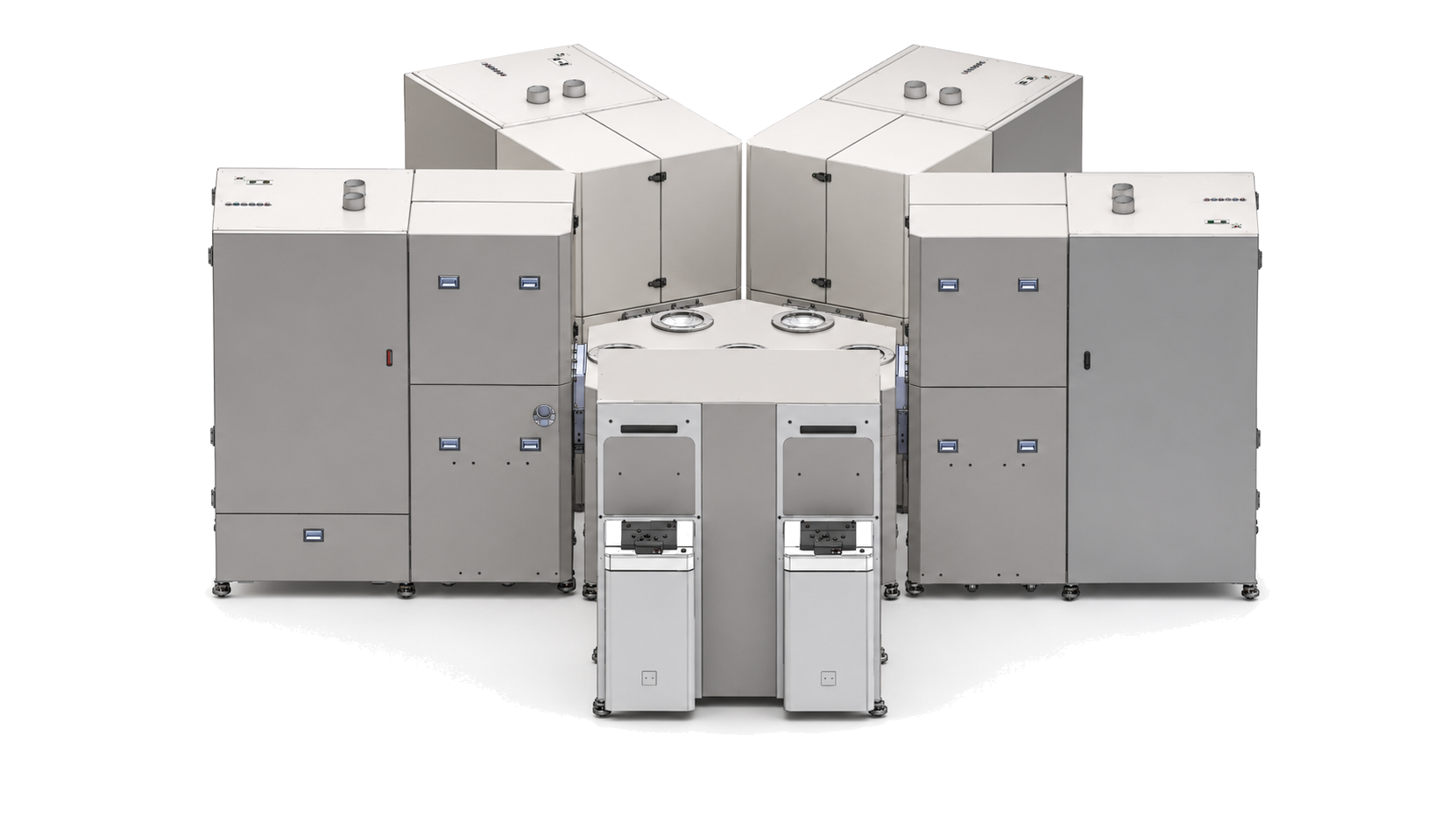
Equipment Specifications
Designed from the ground up for high-volume 2D TMD manufacturing — precision, reliability, and serviceability built in at every layer.
| Supported materials | MoS₂, WS₂, MoSe₂, WSe₂ |
|---|---|
| Growth temperature | < 450 °C adjustable |
| Growth window | 60 s per monolayer cycle |
| Monolayer growth rate | 0.65 nm/min, atomic-level precision |
| Process gases | H₂, Ar, S(Se) source, Mo/W source |
| RF power (ICP) | 3000 W max @ 13.56 MHz |
|---|---|
| UV power | 200 W max — in-situ defect removal |
| Chambers | 4 independent, parallel process |
|---|---|
| Wafer size | 12 inch (300 mm) |
| Max throughput | 60 wafers/hr (4-chamber parallel) |
| Susceptor | Rotary, edge-clamp design |
| Chamber access | Lift-up lid, easy maintenance |
| Heating method | Full-line SCR, 6 temperature zones |
|---|---|
| Temperature measurement | Dual-mode: thermocouple + IR camera |
| System power | ~35 kW — three-phase AC 380 V, 50/60 Hz |
| Footprint (W × D × H) | 4200 × 3600 × 2200 mm |
From Memory to Aerospace
The platform of choice for next-generation 3D monolithic integration across memory, logic, and radiation-hard silicon.
Monolithic 3D SRAM for next-generation cache architectures with high bandwidth and minimal power.
Cost-effective on-chip DRAM replacement for memory-intensive AI and HPC workloads at extreme density.
Resistive RAM arrays for neuromorphic computing and ultra-dense non-volatile storage.
Magnetic RAM with superior endurance and retention for enterprise and industrial applications.
Memory and compute hardened against cosmic radiation for satellite and aerospace computing.
2D TMD channels for mainstream logic beyond silicon's physical floor — grown directly in BEOL.
Full-Service Partnership
PhantaField is committed to peak equipment performance through the tool's entire operational lifetime.
5-Year Parts Replacement
Replacement of any parts within 5 years to ensure long-term stable operation of the equipment.
Upgrade & Iteration Support
Continuous software and hardware upgrades keep your tool at the forefront of 2D materials technology.
Process Development Service
One on-site equipment engineer and one process engineer assist with 2D TMD CMOS and 3D monolithic integration flows.
Evaluate the NanoGalaxy PPMOCVD
Talk to our process engineers about your 2D TMD integration roadmap, request budgetary pricing, or schedule an on-site demonstration.
Configuration-specific pricing with delivery and installation timeline.
Witness a full 12-inch MoS₂ growth cycle on your own wafer lot.
BEOL thermal-budget and facility-requirements assessment with our engineers.