2D SemiconductorsThe transistor era after silicon — one molecule thick.
What Is a Two-Dimensional Material?
A 2D material is a crystal that is fully functional at a thickness of a single unit cell — a sheet of atoms that behaves like a complete, perfect solid.
Within the plane of the sheet, atoms are joined by strong covalent bonds — the same bonds that make diamond hard. Between sheets there is no bonding at all, only weak van der Waals attraction. That asymmetry is the entire trick: each layer is a chemically complete crystal with no dangling bonds on its surface, so a single layer can be peeled off, grown, or stacked on almost anything without defects forming at the interface.
The field began in 2004, when graphene — a single layer of carbon — was first isolated and shown to conduct electrons ballistically (the 2010 Nobel Prize in Physics). But graphene has no bandgap: it can never switch off, so it cannot make a transistor. The breakthrough for computing came in 2011, when the first monolayer MoS₂ transistor proved that a semiconducting 2D crystal could switch with an on/off ratio above 10⁸.
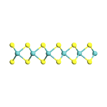
MoS₂ belongs to the transition-metal dichalcogenides — the MX₂ family — where one plane of a transition metal (molybdenum or tungsten) is sandwiched between two planes of a chalcogen (sulfur or selenium). Three atomic planes, 0.65 nm thick, shown in the lattice animation here. Confining electrons to that plane changes the physics itself: the bandgap becomes direct, mobility reaches ~200 cm²/V·s, and the gate sits close enough to command every atom of the channel.
Perfect Electrostatics
In a 0.65 nm channel the gate field reaches every atom — there is no buried bulk where leakage paths can hide. Electrostatic control survives gate lengths where silicon fins collapse.
Dangling-Bond-Free Surfaces
Van der Waals surfaces carry no broken bonds, so monolayers stack on finished wafers — including CMOS metal layers — without interface traps. This is what makes monolithic 3D integration possible.
Tunable by Composition
Swap the metal (Mo ↔ W) or the chalcogen (S ↔ Se) and the bandgap, carrier type, and band alignment shift predictably — a material library for n-type, p-type, memory, and photonic roles.
Why 2D Beats Silicon at the Limit
Silicon is running out of room. At 2 nm and below, quantum tunneling and short-channel effects erode every performance gain. Two-dimensional transition metal dichalcogenides (TMDs) solve this structurally: the active channel is one molecule thick, so electrostatics stay perfect no matter how short the gate gets. PhantaField grows these atomic sheets by MOCVD and stacks them directly into GPU logic — delivering 525× the weight bandwidth of an HBM-based GPU at a fraction of the energy per token.
Atomic-Scale Thickness
2D TMDs are just 3–7 atoms thick — roughly 0.65 nm per monolayer. At this scale, every atom participates in conduction, giving transistors electrostatic control that silicon physically cannot achieve below 3 nm.
Direct Bandgap
Unlike bulk silicon, monolayer TMDs (MoS₂, WS₂, WSe₂) switch from indirect to direct bandgap. This enables efficient light emission and absorption in the same material — unifying logic and photonics in a single atomic sheet.
High Carrier Mobility
Electron mobility in encapsulated MoS₂ reaches ~200 cm²/V·s at room temperature. WSe₂ and MoTe₂ extend this to p-type channels, enabling CMOS-equivalent logic without bulk doping or junction engineering.
Near-Zero Standby Leakage
The semiconducting bandgap of ~1.0–2.0 eV gives on/off ratios above 10⁸ with off-currents of 1 fA/µm. 2D TMD transistors hold a near-ideal ~75 mV/decade subthreshold swing at gate lengths where silicon has long since collapsed.
Why Silicon Has Hit Its Limit
Silicon transistors shrink by thinning the body of the channel. Below ~5 nm, the body can no longer be thinned without destroying the crystal. The result is leakage current that grows faster than performance.
2D TMDs sidestep this entirely. The channel is already at its physical minimum — one unit cell — on day one. Gate length can shrink to sub-1 nm without any body-thinning trade-off, because there is no bulk to thin.
0.65 nm — 8× thinner than the thinnest viable silicon fin.
Sub-1 nm gates demonstrated without threshold voltage collapse.
Material Library
PhantaField's process supports four production-ready TMDs, each optimised for a specific transistor role in the GPU stack.
n-channel logic, baseline TMD for NMOS
Bandgap: 1.8 eV (monolayer)
High-mobility n-channel, LED integration
Bandgap: 2.0 eV (monolayer)
Ambipolar & p-channel CMOS complement
Bandgap: 1.65 eV (monolayer)
Memory and synaptic device integration
Bandgap: 1.55 eV (monolayer)
From Atomic Sheet to Stacked GPU
Growing a 2D layer is only half the problem. PhantaField's full stack covers deposition, integration, and yield — turning a lab material into a manufacturable GPU process.
Plasma-Photon MOCVD Growth
Our proprietary PP-MOCVD reactor grows continuous TMD monolayers across a full 12-inch wafer in under 60 seconds. ICP plasma activation and UV photons break precursor bonds at 350–450 °C — hundreds of degrees below conventional CVD — with production recipes at or below the 450 °C BEOL ceiling.
Monolithic Vertical Stacking
Each TMD layer is grown directly on the dielectric above the previous tier. No wafer bonding, no alignment error, no adhesive. Logic, SRAM, DRAM, and photonic interconnect tiers share clocks and power rails through vertical vias with < 1 ns latency between any two layers.
Heterogeneous Integration
2D TMD logic layers are co-integrated with conventional DRAM and SRAM built in the same fab. The result is a single die carrying compute and memory at 4.2 PB/s of in-tile weight bandwidth — eliminating the HBM bottleneck that throttles today's AI accelerators.
Replacing Today's Bottlenecks
In six existing semiconductor markets, the current solution relies on wafer bonding, hybrid integration, or a separate ASIC driver — all pain points that 2D TMDs eliminate by building logic directly where it is needed.
MEMS Drivers
2D TMD logic can be fabricated directly on MEMS wafers, eliminating the separate ASIC driver die and all packaging. Module footprint shrinks from cm-scale to mm-scale, supply chains shorten, and test moves from post-package to wafer-probe — dramatically cutting cost.
Silicon Photonics
2D TMDs replace the III–V ASIC driver and its bonding process in silicon photonics transceivers. Monolithic vertical vias deliver higher interconnect density, greater bandwidth, lower latency, and reduced thermal dissipation versus hybrid bonding.
CMOS Image Sensors
Backside-illuminated CIS today requires two wafer-bonding steps to stack DRAM and readout circuits. 2D TMD channels grown in-situ eliminate bonding entirely, enabling tighter vertical integration, wider readout bandwidth, and lower noise floors.
3D DRAM
2D TMD leakage current is more than 3 orders of magnitude lower than silicon, allowing capacitor cells to shrink dramatically. Combined with vertical stacking, on-chip VRAM can scale 10–100× beyond today's limits without exotic high-k dielectrics.
3D V-Cache / SRAM
Current Cu–Cu bonding limits V-Cache bandwidth. 2D TMD vias replace bonding pads entirely, delivering 6 orders of magnitude more bandwidth. Multi-layer stacking at 28 nm yields higher SRAM density than cutting-edge 5 nm — at a fraction of the cost.
CPU & GPU Logic
At the 1 nm node and beyond, mainstream CPU and GPU logic will require 2D semiconductor channels. Monolithic compute-plus-memory stacks built from 2D TMDs are the only pathway to continue scaling performance-per-watt after silicon fins hit their physical floor.
New Markets Only 2D Can Unlock
Beyond replacing existing solutions, the unique properties of 2D semiconductors — direct bandgap, dopant-free operation, atomic thinness, and radiation hardness — open entirely new product categories.
AR Displays
Atomically thin TMDs form optically transparent TFT backplanes on transparent substrates, driving see-through near-eye displays with retina-class pixel density and full field of view. This unlocks wafer-thin, fully transparent display arrays that could define the iPhone moment for AR glasses — a projected trillion-dollar market by 2030.
Quantum Computing
Superconducting qubit arrays (Josephson junctions) operate at 10 mK. Silicon drivers require ~100 mK due to dopant freeze-out, forcing wire-bonded standoff interconnects that add noise and cap qubit count. 2D TMDs require no doping and operate at 10 mK, enabling high-density vertical co-integration with qubits — lower noise, larger arrays.
Point-of-Care Biosensors
Graphene FET biosensors (e.g., Cardea Bio, recently acquired) demonstrated the concept. 2D TMD FETs exhibit 74× greater sensitivity than graphene at the same gate geometry. This enables high-throughput, multi-target biosensor arrays capable of real-time concentration monitoring at the point of care.
Aerospace & Space Chips
Ionising radiation creates large-area displacement damage in silicon, permanently degrading performance. In atomically thin 2D TMDs the same dose produces only isolated point defects — orders of magnitude less structural damage. Radiation-hard 2D logic chips deliver longer operational lifetimes for satellites and deep-space missions.