On 21 March 2026, in Austin, Texas, Elon Musk announced a chip fab and did the arithmetic out loud. Tesla and SpaceX would build it, with xAI alongside. Intel joined on 7 April. The long-term goal, in the words SpaceX's S-1 later used, is one terawatt of compute hardware a year. Add up all the fabs on Earth combined, he said, and they come to about 2% of what he needs.
We either build the Terafab, or we don't have the chips
Elon Musk, Austin, Texas, 21 March 2026
He sketched two chip lines: 100 to 200 gigawatts a year for cars and robots, and about a terawatt for space. So 83 to 91% of the output is bound for orbit. The space chip has to live with high-energy ions, photons and electron buildup. Musk also wants it to run hotter than a chip on Earth. In a vacuum, heat leaves only as radiation, and a hotter chip needs a smaller radiator: the area falls with the fourth power of temperature. He had already put a number on it in February: run the chip 20% hotter on the kelvin scale, and since 1.2 to the fourth power is 2.07, the radiator mass halves.
The tool that grows the chip's layers is ours, and so is the chip design described below. We have no announced relationship with SpaceX, Tesla or Terafab. What follows is an open argument about a public plan.
Leading-edge density from a fab with no EUV scanner
The long-term target reported from the Austin launch is a million wafer starts a month. Here is what that means for lithography. The finest features on a leading-edge chip are printed by EUV scanners, machines that use extreme-ultraviolet light. ASML, which makes them, published a planning rule in 2018: one scanner for every EUV patterning step, per 45,000 wafers a month. A 3 nm-class process uses about 19 such steps, and 3 nm-class is a fair yardstick for Intel 14A, the process Terafab has named for full scale.
One million divided by 45,000, times 19, is roughly 420 scanners. ASML ships about 60 a year. That is seven years of its output, for one fab.
A 28 nm fab needs none of them. Density is why a 28 nm fab is normally no answer, though. By analyst estimates, TSMC's 2 nm process (N2) packs about 313 million transistors per square millimeter. A 28 nm process packs about 13 to 14 million. One layer of 28 nm is 22 to 24 times behind.
Sophon, our chip design, is 64 tiers on an ordinary 28 nm silicon base. The tiers hold no silicon transistors. Their transistors sit in semiconductor sheets three atoms thick, mostly molybdenum disulfide (MoS₂). Our NanoGalaxy tool grows the sheets below 450 °C on a finished, wired wafer, whose copper would be ruined at the 1,000 °C that silicon transistors need. The sheets are then patterned with 28 nm-era tools. So the name 28 nm belongs to the base wafer and the toolset, not to the transistors.
Our rule for the stack is simple: divide the node number (the 28 in 28 nm) by the square root of the tier count, memory tiers included. So 28 ÷ √64 gives 3.5 nm-class today, and the 144-tier design planned for 2029 gives 2.3 nm-class.
Counted in transistors per footprint, the picture is more modest. If every tier reached planar density, and the vertical wires between tiers cost no area, 64 tiers would land at about 2.7 to 2.9 times N2. But half the tiers are memory. The fairer comparison sets the 32 logic tiers against N2, where they come to 1.3 to 1.4 times, and sets the memory tiers against the on-chip memory (SRAM) and stacked external memory (HBM) that a 2 nm chip spends its area and energy on.
Per transistor, 28 nm silicon cannot compete, and neither can our tiers. Two-nanometer silicon is roughly three times faster at the same power and spends several times less energy per switch. Each 8-bit multiply in Sophon costs 0.31 picojoules, including reading the weight, against 0.17 to 0.21 in today's leading-edge GPUs.
What the stack changes is distance. Fetching 64 bits from off-chip memory costs 250 to 1,300 picojoules. The multiply that uses them costs a fraction of one. A chip that keeps its weights, the numbers a model has learned, on the die saves far more on the fetch than it loses on the switch. On an 80-billion-parameter model at 8-bit precision, one request at a time, our Sophon whitepaper gives 14,438 tokens a second at 373 W.
The catch is what the 28 nm fab needs instead of scanners: 64 tiers grown and patterned on a tool that does not yet run at volume. The case for the stack rests on that tool more than on the scanner count.
No HBM to buy, no CoWoS to queue for, and a shorter supply chain
On SpaceX's 4 August call, Musk said the biggest constraint right now is memory. Production grows about 20% a year, demand about 200%. Epoch AI's breakdown of an NVIDIA B200 GPU shows why that bites. The chip costs about $6,250 to build. HBM, the memory stacked beside the processor, is $2,900 of it. CoWoS, the packaging that sets the memory beside the logic, is $1,100. Parts ruined in packaging are another $1,000. The two logic dies are $900. Memory and packaging are about 80 cents of every dollar. A fab that makes only the logic die makes the cheap part.
HBM is also its own industry: three makers, in Korea, Taiwan and Japan. The International Energy Agency expects the memory shortage to last through at least the end of 2027. Terafab's own plan includes memory chips. But an HBM stack is 8 to 16 memory (DRAM) dies piled on a logic base die, wired through holes drilled down the stack, and set on a slab of silicon beside the GPU. For the HBM4E generation due next year, that base die is itself 3 nm-class. That means a DRAM process, a stacking line and a second supply chain. A logic fab gets none of them for free. CoWoS is a queue of its own: TSMC's chief executive said in July 2026 that its packaging capacity is so tight it limits customers' growth, and reported lead times run a year or more.
Sophon's 32 memory tiers are 330 GB of two-transistor, no-capacitor (2T0C) DRAM, grown by the same tool as the logic. Because the memory sits in the stack, there is no interposer and no CoWoS step at all. They pack about 440 MB per square millimeter. SRAM, as Cerebras lays it out across a wafer, is about 1 MB. Weights reach the arithmetic at 2.1 PB/s, about 95 times HBM4's 22 TB/s.
Two catches. The die itself is not cheaper. Adding 64 grown tiers, at a 41% combined yield (the share of dies that come out working), puts it at $8,358, more than Epoch's $6,250 for a whole B200. What the die buys is a shorter bill: no HBM line, no CoWoS line, no second supplier to qualify, and no place in the packaging queue.
Capacity has limits too. Cerebras, which builds a wafer-sized chip, already holds 44 GB of SRAM on it and streams weights in from outside for models bigger than that. Sophon's 330 GB holds a 405-billion-weight model stored at 4 bits per weight, about 203 GB, but not at 8 bits, and a trillion-weight model spreads across several dies. For the models that fit, the memory arrives with the logic, from one tool.
Far fewer memory bit flips in orbit
Google's Suncatcher paper, its study of running TPUs in orbit, is usually quoted by halves. Google put a Trillium TPU, its AI chip, into a proton beam. The dose matched a 650 km orbit behind about 10 mm of aluminum: about 150 rad a year.
The first half: the HBM stacks were the most dose-sensitive part. They showed irregularities after 2 krad, and errors their error correction could not fix halted the chip roughly 3.4 times per chip-year (once per 44 rad).
The second half: the most common errors were silent ones. Wrong bits appeared in the core logic and on-chip SRAM with no alarm raised, roughly nine per chip-year (once per 17 rad). Google called that rate likely acceptable for inference, which is serving answers, and left training an open question.
Nothing here says off-the-shelf parts fail in low orbit. Starcloud has flown an NVIDIA H100 GPU and Google is flying four TPUs. What the record does say is that conventional memory gets worse with heat. NASA and JPL's report on DDR4, the ordinary memory in servers, notes that cell leakage roughly doubles for every 10 °C, so radiation-weakened bits stick sooner. That is awkward for a chip meant to run hotter.
Sophon's memory cell behaves differently, and the reason is geometry. A conventional DRAM cell stores its bit in a capacitor sitting over a junction in the silicon, and that junction collects stray charge from about a micrometer of bulk silicon beneath it. Our whitepaper puts the charge that flips such a bit, its critical charge, at around 2 femtocoulombs (fC). Sophon's 2T0C cell flips at about 1.5 fC, which sounds worse. But the only matter in the cell that can collect charge is two transistor channels, each 0.65 nm thick, sitting on insulator. What protects it is how little there is to hit.
The most ionizing cosmic-ray ion deposits about 0.74 fC crossing a channel head-on, half the critical charge. So a flip, an upset in the trade's word, needs a grazing hit, within about 7.6° of the channel plane for an iron ion. Against the cosmic-ray spectrum in GEO, geostationary orbit, the whitepaper's sum comes to at most 2.6 flipped bits a day across all 330 GB. The same sum gives one 288 GB HBM4 GPU 230 to 2,300 a day. And a flipped bit lives at most a second, because the once-a-second refresh passes every word through error correction. The refresh is also a repair.
Lifetime is a separate question from upsets. Komsa showed in 2012 that knocking an atom out of a sheet three atoms thick leaves an isolated point defect, a single missing atom. Krasheninnikov's 2020 review explains why: the avalanche of knocked-loose atoms that a strike sets off in bulk silicon has nowhere to develop in a sheet.
In 2019 Vogl found negligible change in devices built on these sheets after gamma, proton and electron doses equal to many years in low orbit. A Fudan University radio built on one such sheet has run nine months at about 517 km with a bit error rate below 10⁻⁸. It is a radio rather than a memory.
The caveats. The oxide under the sheet still traps charge, Krasheninnikov's review warns, so a device is only as tough as its insulator. A beam test has to settle that along with the upset rate. No maker has published heavy-ion or proton upset data for any capacitor-less 2T0C cell, and our rates cover the memory cell in geostationary orbit only. The logic tiers, and low and medium orbits, still need their own.
The 28 nm base tier is ordinary bulk silicon. It carries the controller and the input/output wiring, so it keeps the exposure of any commercial part to upsets and to latch-up, a radiation-triggered short. In its favor, 28 nm bulk silicon has survived megarad-class total doses in published tests, and the base holds no weights and does no arithmetic. Finally, Sophon's DRAM loses its contents on power-off, so an eclipse, when the array goes dark, needs storage or checkpoints.
29× less compute hardware to launch per gigawatt
SpaceX's filed target is 100 kW of compute per tonne launched, or 10 kg of spacecraft per kilowatt. Now weigh the computer. An NVIDIA GB200 NVL72 rack is about 1,360 kg for 120 to 132 kW, about 11 kg per kilowatt. The silicon of all 72 GPUs weighs roughly 0.3 kg. The copper cold plates that carry heat off the chips are on the order of 100 kg. Racks, pipework, coolant pumps and structure make up most of the rest.
Starcloud's own whitepaper puts about 300 such racks in one 100 t heavy-lift payload and calls for rack-level mass savings. At 1,360 kg each, stock racks would weigh about 408 t, four times the payload.
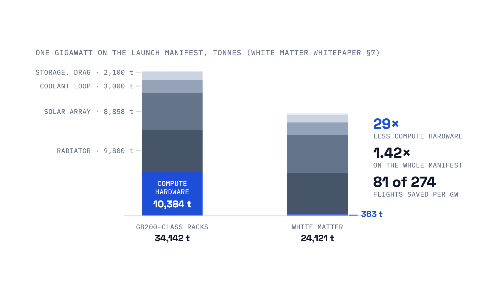
White Matter is our packaging answer: a sealed brick of 40 liquid-cooled silicon plates bonded together, 404 kW in 1.76 liters, about 6.25 kg a brick. For a gigawatt, its whitepaper puts compute hardware at 15.5 t of bricks, or 363 t with frames and power busbars, against 10,384 t of racks. That is 10,021 t saved, 81 of the 274 flights a gigawatt would take.
The rest of the launch manifest is identical whichever computer flies. The radiator, about 1.4 km² at 7 kg/m², weighs about 9,800 t. The solar array weighs about 8,858 t. Add energy storage for eclipse, the loop that carries heat to the radiator, and propellant against drag, and the shared load is 23,758 t. Even the lighter manifest lands near 24 kg a kilowatt against SpaceX's filed 10, and the excess is radiator and array.
The radiator law from the opening, area falling with the fourth power of temperature, has no length, volume or density term, so a denser package shrinks no radiator. Against stock racks, which Starcloud itself says need slimming, the compute-hardware advantage is 29× and the whole-manifest advantage 1.42×. The whitepaper also lists open orbit problems, latch-up and fluids in vacuum among them.
The lever on the radiator is temperature. A 2T0C cell holds its bit for 1.8 s at 25 °C and 28 ms at 85 °C. The refresh that keeps it alive costs 0.08 W at 25 °C and about 4 W at 85 °C, so the stack can run hot cheaply. Sophon's transistors sit at 44 °C on a cold plate while it generates text. That leaves some 40 kelvin of room below the 85 °C just priced for the coolant to rise toward where Musk wants it.
Energy per token is the other lever, with a condition. Serving one request per chip on an 80-billion-parameter model, the whitepaper puts Sophon's energy per token about 174 times below an HBM4-class GPU's. But a GPU normally serves a couple of hundred requests at once, and that sharing closes nearly all of the gap, to within about 30%, though each request then runs at about 300 tokens a second against Sophon's 14,438. In orbit, the energy case is for work that needs one fast answer at a time.
What this means for Terafab
Those are the four points, each with its catch. None of this has been measured on finished silicon: the performance and upset figures are design numbers from the published whitepaper. Heavy-ion and proton beam tests of first silicon are the stated next milestone, ahead of a planned 2027–28 on-orbit test, and White Matter is at concept feasibility, sizing grade, meaning sized on paper and not yet built. SpaceX chose NVIDIA's Vera Rubin hardware for Starmind, its first compute satellites, and SpaceX's own S-1 calls Terafab very early stage. Neither is a decision about 28 nm. The choice is Terafab's to make. What we offer toward the stated goal, a terawatt a year of chips that tolerate space and run hot, is a route that waits on no EUV scanner, only on our own tool.
On that stage in Austin the sum was fabs against need, and need won by fifty to one. We think the arithmetic changes when wafers stop being counted one layer at a time.
Frequently asked questions
- Is PhantaField working with Terafab, SpaceX or Tesla?
- No. PhantaField has no announced relationship with any of them. Terafab is a Tesla and SpaceX initiative with xAI and Intel, and SpaceX's S-1 calls it very early stage, with only a general framework agreed. Its stated full-scale process is Intel 14A, its Giga Texas prototype fab is reported as 2 nm-class, and SpaceX has chosen NVIDIA Vera Rubin hardware for its first orbital compute satellites, targeted for 2027. This post is an open engineering argument about what the publicly stated goal would require.
- Are you saying a 28 nm transistor is as good as a 2 nm one?
- No. Per transistor, 2 nm silicon is roughly three times faster at the same power and spends several times less energy per switch, and in a single layer it is about 2.4 times cheaper per transistor. The claim is about the stack: 64 tiers of atom-thin semiconductor transistors grown on a 28 nm base wafer with 28 nm-era tools. On analyst estimates that puts density per footprint at about 2.7 to 2.9 times TSMC's 2 nm process (N2) if every tier reaches planar density, or 1.3 to 1.4 times logic-to-logic since half the tiers are memory, and it puts 330 GB of memory a third of a micrometer from the logic.
- Has Sophon been tested under radiation?
- Not yet, and no maker has published heavy-ion or proton upset data for any capacitor-less 2T0C cell. Heavy-ion and proton beam tests of first silicon are the next milestone, ahead of a planned 2027–28 on-orbit test. What has been published is the material evidence: isolated point defects rather than the atom avalanches a strike sets off in bulk silicon, in sheets three atoms thick, negligible change in 2D devices after doses equal to years in orbit, and a monolayer MoS₂ radio running nine months in orbit. The insulators around the sheet, which trap charge, are what a beam test must settle.
- Does a denser package mean a smaller radiator?
- No. Radiator area depends on the heat to be shed and the fourth power of temperature, with no term for density, length or volume, so White Matter's 2,900× density gain does not remove a square meter of radiator. It cuts the mass and volume of the compute hardware itself, 29× for a gigawatt, which is 1.42× on the whole manifest once the radiator, array and storage are counted. The way to shrink the radiator is hotter coolant, and the 2T0C cell can run at 85 °C for about 4 W of refresh power.
References
SpaceX, Form S-1 registration statement (Terafab framework; orbital AI compute risk factors; 100 kW of compute per metric ton), US Securities and Exchange Commission, 20 May 2026.
Elon Musk, Terafab announcement remarks, Seaholm Power Plant, Austin, Texas, 21 March 2026 (SpaceX broadcast; verbatim transcript, What's Up Tesla, 28 March 2026); remarks on Intel 14A, April 2026 (Wccftech, 23 April 2026); SpaceX Q2 2026 earnings call, 4 August 2026 (transcript, The Motley Fool); remarks on running space chips 20% hotter in kelvin, Cheeky Pint × Dwarkesh Podcast interview, 5 February 2026 (quoted in R&D World, 25 August 2026).
SpaceXAI and NVIDIA, ‘SpaceXAI Adopts NVIDIA Vera CPU to Accelerate Agentic AI at Massive Scale,’ press release, 24 August 2026.
B. Agüera y Arcas et al. (Google), ‘Towards a future space-based, highly scalable AI infrastructure system design,’ arXiv:2511.19468, November 2025, revised 17 June 2026 (radiation tests re-run; figures cited here are from the revision); T. Beals (Google), ‘Our Project Suncatcher prototype satellite is in orbit,’ The Keyword, 1 October 2026.
E. Feilden, A. Oltean and P. Johnston, ‘Why we should train AI in space,’ Lumen Orbit (now Starcloud) White Paper v1.03, September 2024; Starcloud-1 mission data, Gunter's Space Page.
S. M. Guertin, ‘NEPP DDR4 Radiation Evaluation FY24 Final Report,’ Jet Propulsion Laboratory / NASA Electronic Parts and Packaging Program, 2025.
H.-P. Komsa, J. Kotakoski, S. Kurasch, O. Lehtinen, U. Kaiser and A. V. Krasheninnikov, ‘Two-dimensional transition metal dichalcogenides under electron irradiation: defect production and doping,’ Physical Review Letters 109, 035503 (2012).
A. V. Krasheninnikov, ‘Are two-dimensional materials radiation tolerant?,’ Nanoscale Horizons 5, 1447–1452 (2020).
T. Vogl et al., ‘Radiation tolerance of two-dimensional material-based devices for space applications,’ Nature Communications 10, 1202 (2019).
L. Zhu et al. (Fudan University), ‘Radiation-tolerant atomic-layer-scale RF system for spaceborne communication,’ Nature 650, 346–352 (2026).
V. Somala, ‘NVIDIA's B200 costs around $6,400 to produce, with memory accounting for half,’ Epoch AI Data Insight, 10 December 2025.
International Energy Agency, Key Questions on Energy and AI, World Energy Outlook Special Report, April 2026.
TSMC, Q2 2026 earnings call remarks by C. C. Wei on advanced-packaging (CoWoS) capacity and lead times, July 2026, as reported.
ASML, SMALLTALK 2018 investor presentation (Form 6-K, exhibit 99.4), slide ‘EUV estimated demand per fab by market,’ 8 November 2018; ASML Q1 2026 earnings call, 15 April 2026.
S. Jones, ‘IEDM 2024 – TSMC 2nm Process Disclosure – How Does it Measure Up,’ TechInsights, 27 January 2025 (N2 ≈ 313 MTr/mm²); WikiChip, ‘28 nm lithography process’ (TSMC 28 nm ≈ 13 MTr/mm²).
N. P. Jouppi et al., ‘Ten Lessons From Three Generations Shaped Google's TPUv4i,’ ISCA 2021, Table 2 (energy per operation and per memory access).
PhantaField, ‘PhantaField Sophon Whitepaper,’ Rev 4.1, June 2026 — radiation tolerance §10; retention and refresh versus temperature §6 and §11.2; per-token economics and batch analysis §9 and §5.A.5c. phantafield.com/whitepaper
PhantaField, ‘Project White Matter Whitepaper,’ WM-WP-001, August 2026 — §7, the payload case for orbit. phantafield.com/whitepaper/white-matter