In the first week of November, Sam Altman changed his name on X to Ram Altman. Someone suggested it, and he took it.
It started on a podcast. He told John Collison that with the world’s DRAM this short, it’s a poor thing to keep in everyone’s own computer, where it’s busy about 5% of the time. PC builders did not take that well. He says it was taken out of context. To be fair, he was talking about running AI models at home, and he says he’s been arguing for more memory production for a long time.
Then he wrote this on X:
i want you to have so much ram / lets build more
Sam Altman, on X
OK, Ram. Let’s.
We’re PhantaField. Van der Waals is our design for a 3D DRAM grown one layer at a time. We think we can grow the memory you’re asking for. By our estimate it would cost much less to make than this market charges, and two of its three formats would run much faster than today’s HBM4. We haven’t built it yet, and our first volume is planned for 2029. The numbers follow, including the ones that don’t flatter us.
Who’s going to build it
Collison asked you the obvious question on that podcast. The cure for high prices is high prices, so new memory makers should be pouring in. You told him the invisible hand was failing.
You told him why, too. For a long time, you said, a DRAM maker would invest $20 billion to make $19 billion, and they all remember it. We think you’re right. A company that remembers that won’t overbuild on a letter of intent.
So some of the new memory can come from someone who isn’t a DRAM maker.
Sam, we’re the hand.
What you’re asking for
In October 2025 you signed letters of intent with Samsung and SK hynix in Seoul. OpenAI’s announcement targeted 900,000 DRAM wafer starts a month. Analysts cited by Tom’s Hardware put 2025 DRAM capacity at about 2.25 million wafers a month, so that’s up to 40% of the world’s DRAM wafers. SK Group said it was more than double the world’s HBM capacity at the time.
Those letters aren’t orders. You were back in Korea on 31 October, and no new deal was announced. Samsung says its HBM for 2027 is sold out. SK hynix says its DRAM and HBM are effectively sold out through 2029. Meanwhile, memory has become very expensive.
Conventional DRAM contract prices rose 93–98% in the first quarter of this year alone. HBM4 reportedly sells for about $16 a GB this half. Samsung is reportedly asking about $36–38 a GB for 2027. Micron’s gross margin last quarter was 86.8%.
Memory that takes no DRAM wafer
HBM, the stacked memory beside an AI GPU, starts as DRAM wafers. Each stack is twelve or sixteen thinned dies, drilled and bonded one onto the next. Ours would be grown instead.
Each layer, which we call a tier, is 0.35 µm thick. A stack of 48 comes to 16.8 µm, thinner than a sheet of paper. Our own tool, NanoGalaxy, would grow the tiers on a silicon base. They’re drawn at 28 nm design rules, so the tiers themselves need no EUV scanner.
We’ve designed the memory three ways. Side is one die for an HBM5-class site, the spot beside the GPU where a stack sits. Bond is six tested tiles bonded under each GPU die, and a failed bond scraps that GPU. Grown is tiers grown on the GPU wafer itself.
Growing it changes the wafer math. One wafer of our Side die should yield about 383 good dies if 99.7% of tiers come out good. Each holds 64 GB, so that’s about 24.5 TB. A wafer of current DRAM holds about 3 TB, by our estimate. HBM3E takes about three times the wafers per bit, and Micron expects that ratio to rise. That leaves about 1 TB.
So if all 900,000 wafers went to HBM, about 37,000 wafers of ours would hold the same bits.
That doesn’t make it 24 times cheaper. Each of our wafers would go through growth and patterning 48 times. We expect that to take 240–384 rounds of lithography, and a whole 3 nm chip takes about 90. That’s where our cost comes from, about $176,000 a wafer before packaging and test. It’s also where the time goes. At the pace we assume for Grown, each wafer would spend 240–576 days in the fab.
What the wafer math does mean is that every GB we make would add to supply. Nobody’s laptop would have to give it up.
Cheaper to make than this market charges
You’ll check this, so we’ll be exact.
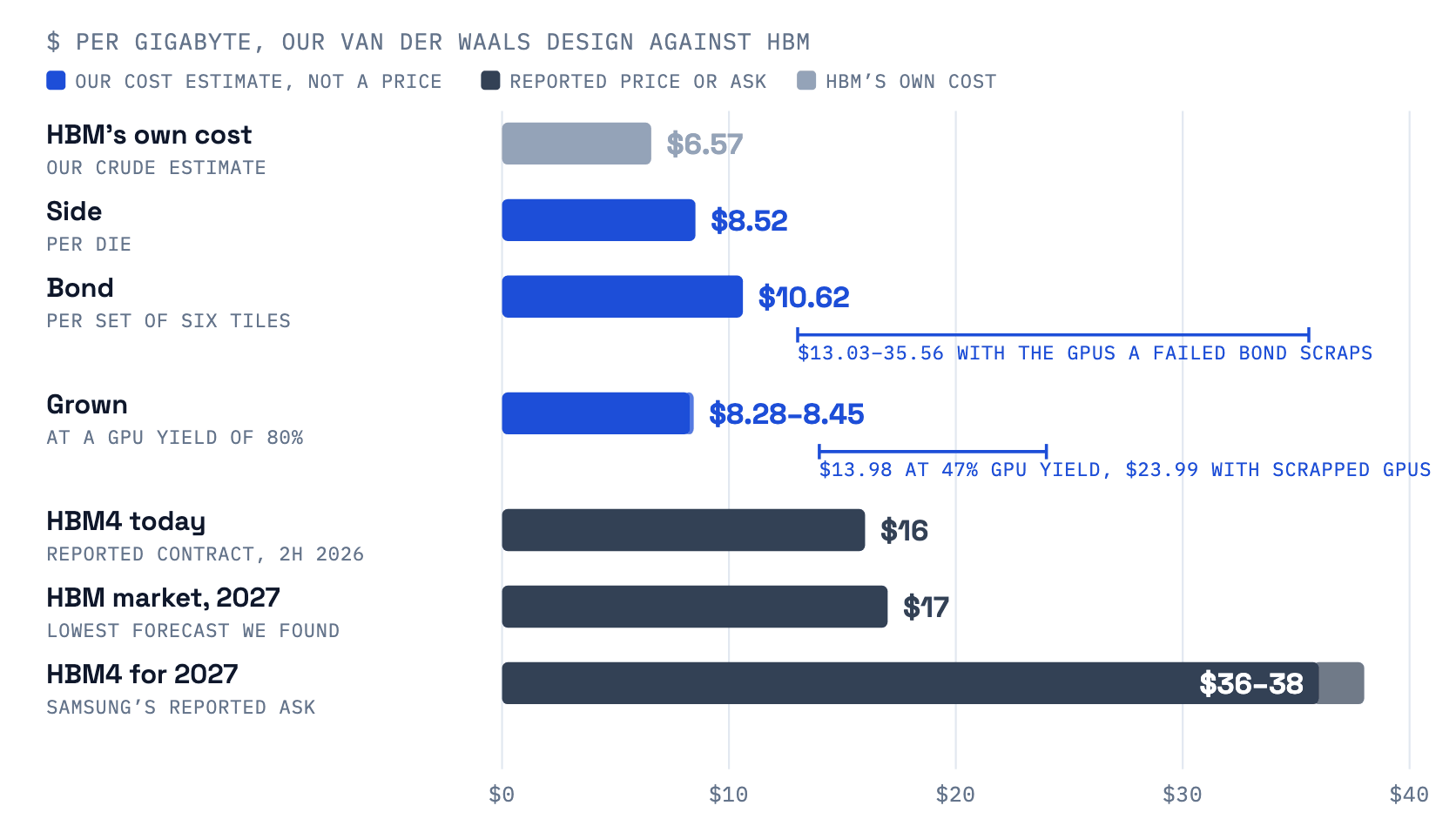
We estimate Side would cost $8.52 a GB to make, about half of HBM4’s $16. Bond comes to $10.62. Count the GPUs a failed bond scraps, and Bond rises to $13.03–35.56. That values a GPU at $5,000–20,000, with a bond yield of 0.98 down to 0.80.
Grown would run at the foundry that makes your chip, on your wafers, so you’d carry the tier cost and the yield. If a tier costs that foundry what it would cost us and 80% of the GPUs are good, Grown works out at $8.28–8.45. If only 47% are good, which is what an 800 mm² die gets at the defect density we design to, it’s about $14. Both figures count on switching a failed tier out for a spare. Without that, and counting scrapped GPUs, it’s as much as $23.99.
All of those rest most on two numbers we can’t yet back with data. One is $3,600 for each tier on a wafer, which has no real process flow behind it, and a leading-edge line may well cost more. If it doubles, Side costs $15.60, about what HBM4 sells for today, and Bond and Grown cost more than that. The other is that 99.7% of tiers come out good. At 99%, Side costs $11.40 and Bond $13.90.
These are costs, not prices, and we won’t publish a price list in a blog post. There’s room below $36, though Bond’s worst case leaves only 44 cents. That $36 is an asking price, and the lowest forecast we found for the whole HBM market in 2027 sits near $17. Side, Bond’s $10.62 and Grown’s $14 clear even that. The worst scrapped-GPU cases don’t.
Last month we wrote that we won’t sell Van der Waals on dollars per GB, because it doesn’t cost less to make than HBM. It still doesn’t. Our crude estimate is that HBM costs its makers about $6.57 a GB. Before scrapped GPUs, and with Grown at a GPU yield of 80%, ours runs 1.3 to 1.6 times that. The selling part we’re changing, for as long as this shortage lasts. HBM’s makers don’t sell at cost. You pay them a price set by a shortage, and the gap between that price and our cost is what we’re talking about here.
It may not last. Side’s volume is planned for the second quarter of 2029, Bond’s for 2030 and Grown’s for 2031. Samsung told investors the tight market runs through 2028, which would end it before any of them. SK hynix says demand stays above supply through 2030, which would give Side under two years of it and Grown none. In the next downturn, plain DRAM would sell for less than our memory costs to make. We say so in the whitepaper. HBM’s makers could price below that cost too.
The RAM in people’s PCs can stay with the DRAM makers. We want the memory under and inside your chip, where speed is worth paying for.
Faster than today’s HBM4
A current flagship GPU die gets 144 GB of HBM4. It reads that memory at 11 TB/s. Your own chip, Jalapeño, does better, with six stacks moving 15.4 TB/s to one compute die.
Bond would hold 352 GB under each GPU die. It would move 61.4 TB/s, which is 5.6 times the flagship and about 4 times Jalapeño. It would keep that pace with its memory as hot as 105 °C, at a 20 ns row cycle, the time to read one row and start the next. At 40 ns and that heat, it would fall to 26 TB/s.
Grown would hold 416 GB inside an 800 mm² die. It would move 209 TB/s with its memory at 95 °C, which is 19 times the flagship and about 14 times Jalapeño. That needs a 20 ns row cycle too, and lanes from the memory into the GPU at 406 MHz or more, against a 500 MHz design rate, unmeasured.
Grown’s catches are the foundry and time. No foundry has qualified an outside company’s process at N3, N2 or A16, and at older nodes it has taken 6–10 years. The tiers would also add 245–588 days to a GPU wafer’s trip through the fab.
Today’s GPUs can’t take all of that bandwidth. We estimate the processors on an earlier flagship die can take in about 33 TB/s at most, however fast the memory. A chip would have to be designed around this memory, with data placed over the processors that read it.
Side goes the other way. It would fill one HBM5-class site with 64 GB and aim for 4.1 TB/s, less than HBM5 will give. On the 28 nm base we priced it on, the edge circuits vendors list today give 2.2 TB/s. Side is mostly for supply. Its 64 GB beats the 36 GB in today’s stacks, but a planned HBM4E stack would hold as much, and one roadmap has HBM5 at 80 GB.
Bond’s and Grown’s multiples are against today’s memory. Our roadmap has Bond in 2030, and HBM5 should be out by then. Reports on its speed don’t agree. One puts it near 8 TB/s a stack, and four stacks would give a die about 32 TB/s. That cuts Bond’s lead to about 2×, and Grown’s to about 6×. Samsung’s target can also be read as about 16 TB/s a stack. That would put HBM5 ahead of Bond and leave Grown about 3× ahead. A finer base could double Bond’s bandwidth, with more heat at the GPU.
Now put cost and speed together. At this half’s price, the HBM4 on a flagship die costs a buyer about $209 for each TB/s it moves. At our crude estimate of what its makers spend, that’s about $86. On a chip built to take everything our memory moves, Bond would cost about $61 to make. Grown would cost about $17 at a GPU yield of 80%, and about $28 at 47%. Count scrapped GPUs, and Bond is $75–204 and Grown $23–48. On an earlier flagship die that can take in about 33 TB/s, Bond is about $113 and Grown about $105, under the $209 but over the $86.
The bill per die still goes up. Bond’s six tiles would cost about $3,700 to make, and a current flagship die’s 144 GB of HBM4 sells for about $2,304 this half. For the higher bill you’d get 2.4 times the memory. Your own Jalapeño carries 216 GB, which would sell for about $3,456. Bond’s cost to make is close to that bill, and it would hold about 1.6 times as much.
Bond would also move a bit for 6 to 48 times less energy than HBM4, before the logic in its base. The catch is heat. Bond’s own heat crosses the GPU to reach the cold plate. At full speed on our target link, the GPU would run 4.1–10.2 K warmer, and at least 11.6 K on the less efficient link behind that 6 times. Grown pays too, at 4.3–6.6 K.
You’re one of the few who can say yes
Side needs a GPU with an HBM5-class controller, and HBM5 isn’t published yet. Bond and Grown ask for more. The chip has to take its power from the front, and its maker has to build for our memory.
With Bond, all of the GPU’s current and off-package signals would run up through our tiles, up to 1.8 kA per polarity on the roughly 800 mm² die our 352 GB assumes. No GPU maker has accepted that yet, and a short there kills the GPU. The foundry that makes your chip would also have to place our tiles on your wafers, and there’s no public precedent for that at TSMC.
Most memory buyers can’t ask a chip designer for that. You can, because you design your own chip with Broadcom. A January report put your second generation on a process powered from the back, which Bond as designed wouldn’t fit. That chip is reported to be months from tape-out, and design work on a third has begun. Bond fits front-powered dies of roughly 2028–2030, so the window is narrow. The time to talk is now, about the generations after the second.
What we’re asking you for
First, where we stand. The material in our tiers, MoS₂, has been measured. It’s a semiconductor grown in sheets a few atoms thick. Its transistors have been measured too, and so has a two-transistor memory cell with a MoS₂ write transistor over a silicon read transistor. The all-MoS₂ cell every tier needs is modeled from those results. So are the capacity, bandwidth, heat, yield, cost and energy figures in this post. We have no hot retention, row-cycle, endurance or soft-error data on that cell yet. We haven’t yet built a memory tier, a bonded part or tiers on a GPU, and no failed tier has been switched out for a spare.
We don’t have a factory yet. About 37,000 wafers a month is a very large line, and nobody builds one on a promise.
Our roadmap has Side in pilot lots from 2027 and in volume from the second quarter of 2029, if the all-MoS₂ cell, a thermal test of the growth steps and tier switching pass first. Bond follows in 2030 and Grown in 2031. Those are planning dates, and we’d fix Bond’s and Grown’s with a GPU maker.
So the ask is simple. Your announcement named a target of up to 900,000 wafers a month at two companies. Give us one percent of those bits. If those wafers were all HBM, that’s about 370 of our Side wafers a month. We’d get there over years, as we add lines, and a firm commitment is what would let us add them sooner. For Bond and Grown, the ask is a co-design.
You’ve been flying to Korea. Our office is in Santa Clara. Write to us at info@phantafield.com, and leave anything confidential out of that first note. Once we’ve both signed a mutual NDA, we’ll tell you which format fits.
Let everyone have so much RAM.
We’ll grow more.
Frequently asked questions
- Is Van der Waals really cheaper than HBM?
- It depends on what you compare. Before scrapped GPUs, we estimate it would cost less to make than HBM4 sells for today, and far less than the price reportedly being asked for 2027. Counting scrapped GPUs, Bond runs $13.03–35.56 and Grown as much as $23.99, and either can top today’s price. It wouldn’t cost less to make than HBM costs its makers: Side, and Grown at a GPU yield of 80%, come to about 1.3 times our estimate of that, and Bond to 1.6 times. Per TB/s of bandwidth, on a chip built to take it and at a 20 ns row cycle, Bond and Grown would cost less to make than HBM4 costs a buyer today. At 40 ns and 105 °C, in the worst scrapped-GPU cases, they wouldn’t. We haven’t published a price.
- Can PhantaField supply 900,000 wafers’ worth of memory today?
- No. We don’t have a factory yet, and we haven’t built a memory tier. Matching it would take about 37,000 of our wafers a month if all those wafers went to HBM, and about 112,000 if they all went to plain DRAM. Our roadmap has Side in pilot lots from 2027 and in volume from the second quarter of 2029. Those are planning dates.
- What do the cost figures leave out?
- Side’s leaves out assembly on the interposer, and so does HBM4’s price. Bond’s leaves out the masks each chip program needs and the GPU maker’s burn-in. A hot retention re-screen after bonding would add $0.24–1.45 a GB. Seven of Bond’s steps are priced with no source behind them, and if they all triple, Bond costs $13.26. Grown’s leaves out the GPU area for its receivers and controllers, and scrap along the line. Its added fab time alone would come to $0.37–0.91 a GB. Who pays for a scrapped GPU is a term we’d have to agree with a buyer. We get HBM’s own $6.57 from a DDR5 contract price of $16.60 a GB, Micron’s 86.8% margin and the 3:1 wafer ratio. It counts no stacking, and that margin covers everything Micron sells.
- What could break the speed and yield numbers?
- If refresh has to run twice as often at 105 °C, Bond falls to about 53 TB/s and Grown to about 63. At 0.8 GT/s, about what the closest reported silicon implies by our estimate, Bond carries 49.2 TB/s against the 1 GT/s we assume. Grown senses through a tier of 2D transistors that hasn’t been measured as a sense latch, and the fallback gives up 5–10% of the GPU die. Its growth has to stay at or below the roughly 400 °C a finished GPU wafer can take, and there’s no tier data at that temperature yet. A GPU-sized tier could also yield worse than the 99.7% we assume. At 93–96%, only 3–11% of good GPUs would survive unless a failed tier can be switched out. Moving data across a die takes power too, so a chip maker would likely cap the memory below these limits.
- Did Sam Altman say people shouldn’t have RAM?
- No. He was arguing about how busy memory stays while supply is short, in a conversation about running AI models at home. He has since written that he wants people to put as much memory in their computers as they like, and that he has argued for more memory production for a long time. We agree with him on that.
- What would OpenAI’s chip have to change?
- For Side, it needs an HBM5-class controller and edge circuits that can talk to a 64 GB die. If HBM5 is 4,096 bits wide, each site also takes about twice an HBM4 site’s edge space. Until HBM5 is published, the fallback is the same die behind the published HBM4 port, at 2 TB/s a site, if its refresh can hide under that port’s timing, which we haven’t shown. For Bond, all of the chip’s current and off-package signals run through our tiles. It must take power from the front of the die, with the pads and memory ports our tiles bond to where its bumps would be, and add 768 channel controllers. Its maker’s line must bond, fill and thin our tiles on its wafers, and each chip program needs its own tile design. Grown needs front power too, a grid for the towers that carry power and signals through the tiers, about 768 channel controllers and the receivers they feed, and a foundry willing to qualify the process. For Bond and Grown, its on-die network has to carry far more than today’s can, or the memory gets capped and the data placed over the processors that read it.
References
Sam Altman and John Collison, ‘Why Sam Altman is against a single superintelligence,’ Cheeky Pint, episode 39, 29 October 2026.
Sam Altman (@sama), posts on X, 3 November 2026. The Tribune (India), ‘Sam Altman publicly embraces the nickname Ram Altman after backlash over comments on PC,’ November 2026.
OpenAI, ‘Samsung and SK join OpenAI’s Stargate initiative to advance global AI infrastructure,’ 1 October 2025. Bloomberg, ‘Samsung, SK Hynix shares leap after OpenAI taps Korea for chips,’ October 2025. The Register, ‘OpenAI ropes in Korean giants Samsung and SK Hynix to feed its AI megaproject,’ 2 October 2025.
TrendForce, ‘OpenAI’s Stargate 900k DRAM wafers could hit 40% of global output,’ 2 October 2025, citing Reuters and Tom’s Hardware. Tom’s Hardware, ‘OpenAI’s Stargate project to consume up to 40% of global DRAM output,’ October 2025, for the analysts’ 2025 capacity estimate.
The Korea Herald, ‘Altman bets on Samsung, SK as AI race intensifies,’ 2 November 2026. CNBC, ‘Sam Altman makes surprise South Korea visit as OpenAI builds on chip partnerships,’ 2 November 2026.
TrendForce, ‘Rapid contract price surge drives 1Q26 DRAM industry up 81% QoQ,’ 1 June 2026.
Seoul Economic Daily, 12 July 2026, reporting DigiTimes contract figures, via Capital & Compute, HBM prices, read November 2026 (HBM4 at $2.00 per Gb in the second half of 2026; 2027 forecasts, including Goldman Sachs near $17 per GB).
The Korea Herald, 7 October 2026, citing local media on Samsung’s 2027 HBM4 asking price, in the mid-to-high $4 range per Gb. An asking price, not a confirmed contract.
Micron Technology, fiscal Q4 2026 results (GAAP gross margin 86.8%), Form 8-K exhibit 99.1, 30 September 2026.
XenoSpectrum, ‘Micron: HBM3E consumes 3× more wafer capacity than DDR5, and the gap will widen,’ 27 August 2026. TechInsights, Samsung D1b DRAM (16 Gb LPDDR5X, 36.68 mm²), for the density and die size in the wafer figure.
TechCrunch, ‘Samsung expects memory shortage to worsen through 2027 and last until 2028,’ 31 July 2026. MoneyToday, ‘Samsung Electronics says memory shortage will persist through 2028,’ 29 October 2026. TrendForce, ‘SK hynix 3Q26 OPM hits record 80%; says DRAM, HBM effectively sold out to 2029, 14 LTA customers signed,’ 28 October 2026. TrendForce, ‘Samsung says HBM share matches DRAM standing as HBM4 sales triple; DS margin hits 72%, 10 LTA clients signed,’ 29 October 2026, for its 2027 HBM being sold out.
OpenAI and Broadcom, ‘OpenAI and Broadcom announce strategic collaboration to deploy 10 gigawatts of OpenAI-designed AI accelerators,’ 13 October 2025. ServeTheHome, ‘OpenAI Jalapeno custom AI ASIC at Hot Chips 2026,’ 25 August 2026. TrendForce, ‘OpenAI debuts Jalapeño AI inference chip, with Samsung reportedly supplying HBM4,’ 26 August 2026, citing Bloomberg on the second generation’s tape-out. TrendForce, ‘OpenAI reportedly to deploy custom AI chip on TSMC N3 by end-2026, second-gen planned for A16,’ 15 January 2026, citing Commercial Times.
PhantaField, Van der Waals: One Memory, Three Ways onto a GPU, whitepaper: §7 for tier yield, §8 for cost, §10 for HBM5, §15 and §16 for Bond, §19 for lithography rounds and fab time, §20 for Grown, §22 for who carries what, §23 for the family table, §24 for what we still have to prove.