Memory · 3D DRAM in Three Formats

Van der WaalsWe designed one memory to go beside a GPU, under it, or into it.

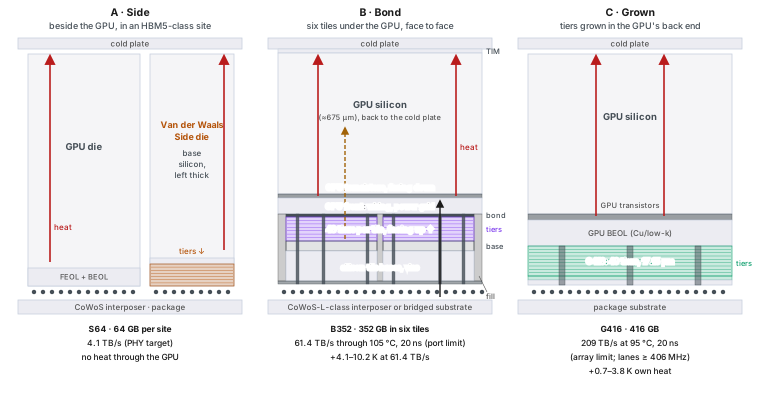
Three schematic cross-sections. A, Side: a Van der Waals die beside the GPU in an HBM5-class site on a CoWoS interposer. B, Bond: six tiles hybrid-bonded under a face-down GPU, carrying its power and I/O to the package; the memory’s heat rises through the GPU. C, Grown: tiers grown between a flip-chip GPU’s wiring and its bumps, crossed by towers; the GPU’s heat still leaves through its own silicon.
Why It Matters

Four reasons, all physical

01

Heat has a short path

A Side die’s 48 tiers are 16.8 µm of memory with no bonded joint between them, so the memory runs within 0.5–1 K of its base. An HBM stack puts twelve or sixteen thinned dies, and as many bump-and-underfill joints, in the same heat path.

02

Thin, with no stacking ceiling

Each tier adds 0.35 µm; nothing is drilled, bumped or thinned per tier. HBM stops at sixteen dies under a 775 µm package height. Here the count is set by the growth’s anneal budget, about 300 tiers with tungsten or ruthenium base wiring, and 300 tiers would stand 105 µm tall.

03

Less energy per bit

Bond moves a bit from cell to GPU receiver for 0.08–0.4 pJ before the base datapath, 6 to 48 times less than HBM4’s 2.4–4 pJ, because the data crosses one bond instead of two PHYs and an interposer. Grown’s cell-to-GPU figure is 0.03 pJ, with its tier-P latch, receivers and ECC excluded.

04

Little for a cosmic ray to hit

The channel is one atomic layer of MoS₂ and the bit sits on a transistor gate, not in a trench capacitor, so a particle strike has almost no volume to deposit charge in. The soft-error rate that leaves is untested: no Van der Waals part has been irradiated.

Three Formats

Pick where the memory goes

The same tiers, three ways, differing in what you buy, what your GPU changes and the heat at the GPU junction, its transistors’ temperature. Bandwidth depends on the row cycle: the time to read a row and be ready for the next.

01 · Beside the GPU

Van der Waals Side S64

A tested die in an HBM5-class site, on the CoWoS interposer.

Capacity
64 GB per siteOne tested die; HBM5 is unpublished (October 2026).
Bandwidth
4.1 TB/s per siteThrough 105 °C at a 20 ns row cycle (PHY target); 2.2 TB/s with listed 28 nm PHY IP.
GPU junction
NoneIts heat leaves through its own site, as an HBM stack’s does.
See Side →
02 · Bonded under the GPU

Van der Waals Bond B352

Under each GPU die, carrying its power and I/O.

Capacity
352 GB per GPU dieSix tested tiles under an assumed 800 mm² die.
Bandwidth
61.4 TB/s per GPU dieThrough 105 °C at a 20 ns row cycle (port limit).
GPU junction
+1.3–4.0 K at 22 TB/sOwn heat; up to +8.6 K with our base datapath and leakage.
See Bond →
03 · Grown into the GPU

Van der Waals Grown G416

Grown on the GPU wafer, under licence.

Capacity
416 GB per GPU dieOn an assumed 800 mm² die.
Bandwidth
209 TB/s per GPU dieAt 95 °C and a 20 ns row cycle (array limit; lanes ≥ 406 MHz, unmeasured).
GPU junction
+0.7–3.8 K from 22 to 161 TB/sOwn heat; +0.3–1.1 K in the towers; +0.5–2.0 K to hold the GPU’s clocks.
See Grown →

HBM gets bigger by stacking more dies. Van der Waals gets bigger by growing more layers, a third of a micron each.

Van der Waals Side · Beside the GPU

We grow 64 GB on one die, with no stacked dies

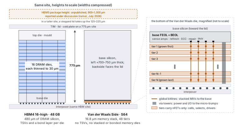
A silicon base with 48 tiers grown on it at 28 nm design rules, flipped into an HBM5-class site like an HBM stack: no through-silicon vias (TSVs), no bonded dies.

Cross-section, heights to scale: a 16-high HBM4 stack of sixteen thinned dies joined by TSVs, and a Van der Waals Side die with its silicon base on top and 48 tiers facing the interposer, in the same 775 micrometre site; a dashed band marks the 900 to 1,000 micrometre height discussed for HBM5.
Side beside a 16-high HBM4 stack, to scale; dashed, the 900–1,000 µm height reported for HBM5 (press reports, July 2026). Whitepaper Figure 5.
S64
Capacity64 GB per site (64 GiB, HBM’s unit); KAIST projects 80 GB per HBM5 stack (June 2025)
Tiers48 (46 data + 2 spare), 16.8 µm on a silicon base; one 126 mm² die, 775 µm tall
Bandwidth4.1 TB/s per site through 105 °C at a 10 or 20 ns row cycle (PHY target: 4,096 pins at 8 Gb/s; listed HBM3E PHY IP reaches 8.0–8.4 Gb/s per pin on 7 and 5 nm-class bases); 2.2 TB/s with listed 28 nm PHY IP; below the speed Samsung has stated for HBM5 (September 2026)
Rated105 °C at a 10 or 20 ns row cycle; 85 °C at 40 ns (throughput rating: after refresh the array still feeds the port; 1.11–1.13× margin at 105 °C and 20 ns at full access efficiency)
Energy per bitn/a: the PHY’s energy depends on the base node (0.25–1.0 pJ assumed)
GPU junctionNone: its heat leaves through its own site
InterfaceA 4,096-bit HBM5-class port, the width and rate KAIST projects (June 2025; other reports differ); HBM5 is unpublished: JEDEC lists it as in development (October 2026); base node free: 28 nm in the cost basis; a 7 nm-class base reaches the 8 Gb/s PHY target with listed IP
Van der Waals Bond · Bonded under the GPU

We put six tiles under the GPU

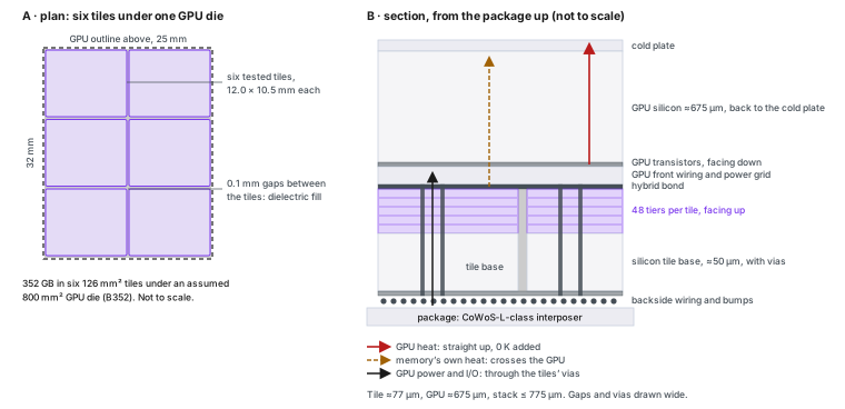
The GPU sits face-down, its silicon to the cold plate, on six tested tiles hybrid-bonded to its front. Vias inside the tiles carry all its power and I/O to the package; the gaps hold only fill.

Two panels. A: six Bond tiles in two columns of three under the GPU die’s outline, gaps filled with dielectric. B: cross-section from the package up: bumps, a tile’s silicon base, its 48 tiers with vias through them for the GPU’s power and I/O, the hybrid bond, the GPU face-down, and the cold plate; the GPU’s heat rises straight up, the memory’s through the GPU.
A: six B352 tiles under an assumed 800 mm² GPU die; B: the GPU face-down. Whitepaper Figure 9.
B352
Capacity352 GB per GPU die, in six tiles under an assumed 800 mm² die (2.4× a Rubin die’s 144 GB)
Tiers48 per tile (46 data + 2 spare), 16.8 µm on a silicon base; six 126 mm² tiles about 77 µm thick
Bandwidth61.4 TB/s per GPU die through 105 °C at a 20 ns row cycle (port limit; 5.6× a Rubin die’s 11 TB/s); at a 40 ns row cycle 61.4 TB/s through 95 °C (port limit) and 26 TB/s at 105 °C (array limit)
Rated105 °C at a 20 ns row cycle or less; 95 °C at 40 ns (refresh duty 50% or less: 38% at 105 °C and 20 ns)
Energy per bit0.08–0.4 pJ, cell to GPU receiver, before our base datapath; 6 to 48 times less than HBM4’s 2.4–4 pJ
GPU junction+1.3–4.0 K of own heat at 22 TB/s (up to +8.6 K with our base datapath and leakage); +4.1–10.2 K at 61.4 TB/s; +0.2–0.3 K to hold the GPU’s clocks through our 0.25% voltage drop. For a 105 °C memory rating the GPU junction over the tiles stays at or below about 98 °C at a 150 W memory budget (94–101 °C at 61.4 TB/s, by link)
Interface491,520 lanes at 1 GT/s across six hybrid bonds, UCIe-3D-class; the GPU’s power and I/O pass through the tiles’ vias; no standard; 2 GT/s on a 12 nm-class base

Via electromigration at 105 °C and link signal integrity are its main risks.
Van der Waals Grown · Grown into the GPU

We grow memory on the GPU wafer itself

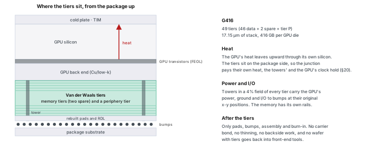
A back-end module the foundry runs on the GPU wafer after its last copper wiring, before its bumps. Towers through every tier carry the GPU’s power and signals.

Cross-section of Van der Waals Grown on a flip-chip GPU, from the package up: substrate, bumps, rebuilt pads, the 49 tiers including a periphery tier, crossed by towers, then the GPU’s copper wiring, transistors and silicon, and the cold plate on top; an arrow shows heat rising from the transistors through the GPU silicon to the cold plate.
Grown on a flip-chip GPU, from the package up: the GPU’s heat still leaves through its own silicon. Whitepaper Figure 10.
G416
Capacity416 GB per GPU die, on an assumed 800 mm² die (2.9× a Rubin die’s 144 GB)
Tiers49 (46 data + 2 spare + tier P, the periphery tier), 17.15 µm, grown on the GPU wafer
Bandwidth209 TB/s per GPU die at 95 °C and a 20 ns row cycle (array limit; lanes at 406 MHz or more, against a 500 MHz design rate, unmeasured; 19× a Rubin die’s 11 TB/s); 161 TB/s at 105 °C; 105 / 80 / 32 TB/s at 85 / 95 / 105 °C and a 40 ns row cycle (array limit)
Rated105 °C at a 20 ns row cycle or less; 95 °C at 40 ns (refresh duty 50% or less: 38% at 105 °C and 20 ns)
Energy per bit0.03 pJ, cell to GPU receiver; the tier-P latch, receivers and ECC excluded, so not ranked against Bond or HBM4
GPU junction+0.7–3.8 K of own heat from 22 TB/s at 85 °C to 161 TB/s at 105 °C; +0.3–1.1 K in the towers; +0.5–2.0 K to hold the GPU’s clocks through their voltage drop. For a 105 °C memory rating the GPU junction under the memory stays at or below about 102 °C at 161 TB/s, about 104 °C at 22 TB/s
Interface4.12 M lanes from tier P into the GPU’s top metal at a 500 MHz design rate (unmeasured); no bond, TSV or PHY; no standard

With no TSVs, gaps or seal rings, each tier keeps 768 of the die’s 800 mm² for cells, against 640 mm² across Bond’s six tiles: the same 46 data tiers hold more, with 20% more sense paths. The furthest out of the three: grown on untested GPUs. At a 20 ns row cycle Bond and Grown deliver more than a GPU takes today: an H100-class die’s SMs load about 33 TB/s from L1 (our estimate).

Side by Side

Three formats against HBM4 beside the die

Per GPU die. Bandwidth at 95 °C and a 20 ns row cycle unless stated, the limiter in brackets; 40 ns figures at 95 °C. Multiples are against a Rubin die’s 144 GB and 11 TB/s.

Side S64Bond B352Grown G416HBM4, a Rubin die’s share
Capacity per GPU die256 GB at four sites (128 at two)352 GB in six tiles (2.4×)416 GB (2.9×)144 GB
Bandwidth per GPU die16.4 TB/s at four sites (PHY target; 8.2 at two); 8.7 TB/s with listed 28 nm PHY IP61.4 TB/s (port limit; 5.6×); 61.4 TB/s at 40 ns (port limit)209 TB/s (array limit; lanes ≥ 406 MHz, unmeasured; 19×); 80 TB/s at 40 ns; more than Bond (note below)11 TB/s
Rated105 °C at a 10 or 20 ns row cycle; 85 °C at 40 ns105 °C at a 20 ns row cycle or less; 95 °C at 40 ns105 °C at a 20 ns row cycle or less; 95 °C at 40 nsn/a
GPU junctionNone+1.3–8.6 K at 22 TB/s; +4.1–10.2 K at 61.4 TB/s (upper figures with our base datapath and leakage); +0.2–0.3 K to hold the GPU’s clocks; at or below about 98 °C at a 150 W memory budget+0.7–3.8 K from 22 to 161 TB/s; +0.3–1.1 K in the towers; +0.5–2.0 K to hold the GPU’s clocks; at or below about 102 °C at 161 TB/sNone
What the GPU maker changesAn HBM5-class controller and PHY that support a 64 GB density, at 4,096 wires per siteA front-side-powered die with a bond array and memory ports, not bumps, and no pads over the gaps or bandOn a front-side-powered die: a landing grid, lane receivers, channel controllers; the foundry qualifies the modulen/a
Tested before it meets the GPUYesYes: tiles and vias before, via continuity after bondingNo: grown on untested GPUsYes
StandardNone: HBM5 is unpublished (October 2026)None (UCIe-3D-class lanes)NoneJESD270-4

Side, a generation after HBM4, is counted at an assumed four sites per die (two, as KAIST’s F400 projection implies, June 2025, halves its figures); its GB are binary like HBM’s. At the same memory temperature and row cycle, for the same cell retention, and with its lanes above 119 MHz, Grown delivers at least 1.1× Bond wherever Bond delivers anything: 3.8 / 3.4 / 2.6× at 85 / 95 / 105 °C and a 20 ns row cycle, 1.7 / 1.3 / 1.2× at 40 ns, from 20% more sense paths, with the same 46 data tiers to refresh.

The Cell

Two transistors, no capacitor

Each bit is a gain cell: one transistor writes a charge onto a second’s gate, which reads it without draining it; no capacitor, no write-back. Fudan University published the same MoS₂-over-silicon design in 2024; the stack is what is new.

Measured
  • The capacitor-less 2T0C cell (a MoS₂ write FET over a silicon read FET) stays readable past 1,000 s and shows about five distinct levels. Van der Waals stores one bit per cell.
  • MoS₂ nFETs, measured in a stack over a silicon p-FinFET.
Not yet measured
  • A cell with both transistors in MoS₂, which every tier needs.
  • Retention and row cycle at 85–105 °C.
  • Nothing bonded has been built, and nothing has been grown on a GPU.
Heat and Refresh

Hot memory refreshes more, in every format

Memory temperature25 °C85 °C95 °C105 °C
Refresh interval1 s20 ms10 ms5 ms
Side S64, mW per GB≈0.50≈25≈50≈100
Bond B352, mW per GB≈0.46≈23≈46≈92
Grown G416, mW per GB≈0.47≈23≈47≈93
HBM self-refresh, for reference23–52, temperature not stated

Per GB sold, design retention, modeled. Per user-capable GB all three refresh alike: ≈0.46 / 23 / 46 / 91 mW. At 85 °C refresh costs what HBM’s self-refresh does; at 105 °C about twice HBM’s top figure. Rises are in kelvin: +1 K is +1 °C.

Grown on NanoGalaxy

Every tier comes off our own tool

Every tier is grown below 450 °C on our NanoGalaxy PP-MOCVD tool, on 300 mm wafers; on a GPU wafer the stack must fit the foundry’s time-at-temperature limit for finished copper wiring, about 400 °C.

The Van der Waals whitepaper

Read the Whitepaper
Hosts

Which GPUs?

Van der Waals Side is designed for an HBM5-class site. HBM5 is unpublished: JEDEC lists it as in development (October 2026), so Side needs a GPU with an HBM5-class controller and PHY that supports its 64 GB density; we will align its port with the standard when it is published.

We designed the Van der Waals bond face for the next generation of AI GPUs, including Feynman, the generation NVIDIA has announced for 2028. NVIDIA has said Feynman will use 3D die stacking and custom HBM. It has not published a bond interface, a memory interface, a die size or a power figure, and it has not said that any memory will be bonded onto its GPU dies. PhantaField has no relationship with NVIDIA. Bonding Van der Waals to a Feynman GPU is our design target, not a compatibility claim: it would need NVIDIA to add a matching hybrid-bond array and memory ports to its die. Our bond face follows the open UCIe-3D class of die-to-die links, so any GPU or accelerator maker can build to it.

FAQ

Questions we get

Is it compute-in-memory?

No. The GPU computes; Van der Waals stores bits. Sophon is our compute-in-memory chip.

Does it replace HBM?

Side fills HBM5-class sites with 64 GB from one tested die, for capacity, not speed: 2,048-bit HBM4E samples carry about 4 TB/s (May–June 2026). Bond and Grown add a near tier under or inside the GPU die, at a cost in GPU junction heat.

What if a tier, tile or die fails?

Spare tiers help only if a failed tier can be switched out, which no format has shown; Grown depends on it. In Bond and Grown a failed bond or a power short through the tiers scraps the GPU.

Van der Waals is a design: the memory cell and transistors are measured; every chip-level figure here is modeled from them. GPU, HBM and industry figures are third-party and dated where they appear.

NVIDIA is a trademark of NVIDIA Corporation. Feynman, Rubin and NVLink are names NVIDIA uses for its products and are used here only to identify them. PhantaField is not affiliated with, endorsed by or sponsored by NVIDIA. CoWoS is a trademark of TSMC. Other product names are trademarks of their owners and are used here only to identify them.

Talk to Us

The Right Format for Your GPU

Tell us your GPU’s HBM sites, die face, power map and process flow; we’ll say which format fits.

Format fit

Side, Bond or Grown for your die.

Thermal plan

GPU junction rise and refresh at your temperatures.

Whitepaper walkthrough

Every derivation, with its engineers.

We use this only to reply to you, and never sell it.